
Two research groups, using very different materials and approaches, have recently fashioned optical and photonic components that they claim are far thinner than previously demonstrated devices. In one study, the authors report creating “the thinnest and lightest solar cells demonstrated to date,” using a flexible organic substrate (Org. Electr., doi: 10.1016/j.orgel.2016.01.022). The other research team leverages the optically intriguing properties of a 2-D material, molybdenum disulfide (MoS2), to unveil what the study bills as “the world’s thinnest optical lens” (Light. Sci. Appl., doi: 10.1038/lsa.2016.46).
Solar cells “light as a soap bubble”
The fabrication process devised by the MIT team reportedly allows solar cells so thin and light they can be draped atop a soap bubble without popping it. [Image: Joel Jean and Anna Osherov]
To create its ultra-lightweight solar cells, the first research team—led by Vladimir Bulović of the Massachusetts Institute of Technology (MIT), USA—focused particularly on slimming down the solar-cell substrate. At present, the most common substrate for photovoltaics is glass, which—while exceptionally smooth and strong—adds substantial weight and rigidity to the solar cell built on top of it. As a lighter and more flexible replacement, the scientists zeroed in on a substrate candidate called parylene-C, an organic chemical that is known to form thin, smooth films, and that is already used commercially as a protective coating in biomedical and electronic components.
The key to the ultrathin cells, however, lies, according to Bulović, not in the specific material but in the method. That method begins with spin-coating a glass foundation with a solvent that acts as a “release” layer to allow for removal of the solar cell. Then, using vapor deposition in vacuum conditions, a base layer of parylene is laid down on the glass, followed by organic solar-cell components, which are finally overtopped by an additional protective coating of parylene. The ultrathin component is then peeled off of the glass.
The fabrication method allows the entire device to be created in a single room-temperature process, without handling the fragile device or breaking the vacuum, minimizing the risks of damage. “The innovative step,” according to Bulović, “is the realization that you can grow the substrate at the same time you grow the device.”
The result of the process, according to the researchers, is “the thinnest and lightest solar cells ever made”—a claim that they demonstrated by draping one of the flexible cells on top of a soap bubble, without popping it (see image above). The team points out that, while the experiments it reports used parylene and organic solar cells, the method should be generalizable to other thin-film materials and photovoltaic components.
The initial component is a proof of concept only, and will require considerable work to boost component efficiency and scale the process to production. Still, the researchers believe that the components, and the process needed to develop them, could ultimately offer a new route to thin, flexible solar-cell films that can be “seamlessly adhered to a variety of solid surfaces to provide additive solar power” to portable electronic devices.
“Atomically-thin” optical lenses
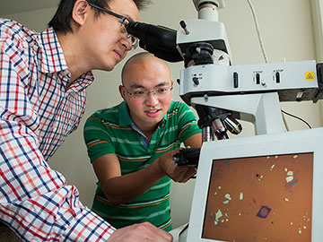
ANU researchers Yuerui Lu and Jiong Yang, with ultrathin lens displayed on video screen. [Image: Stuart Hay, ANU]
Meanwhile, a research team from Australian National University, Canberra, and the University of Wisconsin, Madison (USA), has tested the limits for ultrathin optical lenses, and come up with components that are only a few layers of atoms thick. Their tool was a specific material, molybdenum disulfide—one of the rapidly growing family of “2-D materials” whose best-known member is graphene.
MoS2 has some intriguing optical properties, such as a direct band gap, that set it apart from graphene, and that have already signaled its potential in integrated photonic devices (see “Optoelectronics in Flatland,” OPN, July 2015). But the ANU-Wisconsin team, led by ANU research scientist Yuerui Lu, discovered that single-layer MoS2 also has a “giant” optical path length (OPL), around an order of magnitude greater than that of graphene.
The large OPL is the result, according to the team’s modeling, of strong multiple reflections at the interface between the high-refractive-index MoS2 and other materials such as air and silica. What’s more, the refractive index of multilayer MoS2 can actually be tuned, on the fly, with an externally applied electric field.
The team decided to see if it could put these qualities into service to create what it calls “a new class of optical materials”—one based on phase-front engineering of optical beams in high-index 2-D materials. To fabricate the devices, the researchers mechanically exfoliated monolayer sheets of MoS2, deposited multiple layers on a silica substrate, and then used a focused ion beam system to sculpt the layers atom by atom to create a concave “micro-lens” 10 microns in radius and 6.3 nm thick.
The team was able to characterize the focal length and other optical properties of the lens, which they claim is the thinnest ever devised. Because of that thin profile, and in particular because the refractive index—and, thus, the lens properties—can be tuned with an external electric field, the scientists see promise for the new technique as an enabling technology in miniature cameras, flexible displays and other devices. “Our work here opens an exciting opportunity,” the study concludes, “to use high-index 2-D materials to control the flow of light.”