
 [iStock]
Optical data interconnects are integral elements of modern telecommunications and chip-based computing. There is a need for high-speed, energy-efficient, cost-effective on-chip light sources, photodetectors and optical modulators. As Moore’s law begins to hit physical barriers, the search for alternative post-silicon materials and technologies has intensified. And, although silicon still reigns supreme in microelectronics, it’s increasingly clear that the next leap in nano-optoelectronic technology will come not from fashioning ever-smaller devices from conventional bulk semiconductors, but from using radically new building blocks—such as low-dimensional semiconductors.
The modern trend toward nanoscience and nanotechnology was arguably kick-started by novel instrumentation (such as scanning tunneling microscopy) and by the discovery of 0-D fullerenes and 1-D carbon nanotubes. It was the separation of graphene in 2004 by Geim and Novoselov, however, that marked the onset of the second wave of research in low-dimensional materials. Since then, the discovery of other 2-D materials has only sped up research and development in electronics and photonics, with the ultimate goal of one day replacing silicon with “flat” materials and devices.
In this article, we provide a selective survey of the rapidly growing field of 2-D optoelectronics. After a brief review of the physical properties of some important 2-D materials relevant to photonics applications, we outline the current status of research from the perspective of three specific nano-optoelectronic devices: modulators, photodetectors/photovoltaics and light emitting devices (LEDs), including single-photon sources and lasers. The aim is not to present an exhaustive overview of the state-of-the-art in this rapidly developing field, but rather to provide a flavor of some of the physics and applications that make these materials so exciting and appealing.
The 2-D landscape
Three materials today offer the triad required to realize all 2-D gated optoelectronic devices: graphene, in the role of a metal; transition-metal dichalcogenides (TMDs), in the role of semiconductors; and hexagonal boron nitride (h-BN), in the role of insulators.
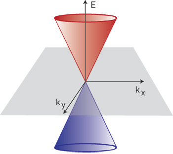 Electronic band structure of 2-D materials: Graphene (metallic). Graphene’s linear dispersion gives rise to “massless” carriers with high mobilities. [Palash Bharadwaj]
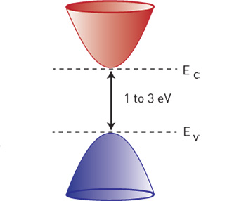
TMD monolayers (semiconducting). TMD monolayers, with a parabolic dispersion and a direct band gap that can vary from roughly 1 eV for MoTe2 to more than 2.5 eV for SnS2, are semiconducting at 300 K. [Palash Bharadwaj]
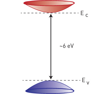 Boron Nitride (insulating). h-BN has a direct band gap of around 6 eV, which makes it an almost ideal insulator at room temperatures and a useful material for deep-UV light sources and lasers. [Palash Bharadwaj]
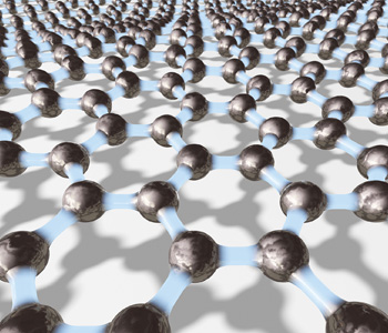
Graphene. The oldest and arguably most common 2-D material, graphene—extremely strong, atom-thick layers of carbon with a 2-D hexagonal lattice structure—was discovered in 2004 by exfoliation from bulk graphite. That discovery came as a surprise, as a truly two-dimensional material had been thought to be thermodynamically unstable and, hence, impossible. Graphene has a unique band structure with linear dispersion, making it a semi-metal with a zero band gap.
One consequence of linear dispersion is that electrons in graphene behave as massless particles, and can exhibit very high mobilities (on the order of 200,000 cm2V–1s–1). Another is that optical absorption in monolayer graphene is nearly constant (about 2.3 percent) for visible and near-infrared wavelengths, and scales linearly with the number of layers. Furthermore, graphene exhibits high optical nonlinearities, which can be exploited for wave mixing and switching.
Transition-metal dichalcogenides. TMDs constitute an entire class of layered materials that, like graphite, can be mechanically exfoliated to yield 2-D monolayers, a feat first accomplished in 2005. They have the general formula MX2 where M is a transition metal like Mo, W, Nb or Sn, and X is a chalcogen, typically S, Se or Te.
TMD bulk crystals typically have an indirect band gap that often transitions to a larger direct gap as the crystal is thinned down to a monolayer—a most curious case of band structure change arising from quantum confinement. The prototype TMD, MoS2, has a direct band gap of 1.9 eV in the monolayer form; single-layer WS2 has a band gap of 2.05 eV, and WSe2 has a band gap of 1.65 eV. The technological and scientific significance of a relatively large direct band gap in these sub-nanometer-thick crystals cannot be overemphasized: it opens the door for realizing photodetectors, solar cells and LEDs, in conjunction with integrated electronic logic circuitry—even, potentially, on flexible substrates.
Another fascinating feature common to the band structures of many TMDs is that of energy-degenerate “valleys” in momentum space, which exhibit selective circular dichroism. This means that electrons in a given valley “talk” to circularly polarized photons of a given handedness only, a trait pertinent for future valley-based computing schemes (dubbed “valleytronics”).
Interestingly, electron-hole pairs, or excitons, in TMDs commonly have a very high binding energy, at roughly 500 meV. By contrast, direct-band-gap semiconductors like GaAs and CdTe have exciton binding energies ranging from 4 meV to 20 meV. As a consequence, the excitonic lifetime in TMDs is very short, of the order of tens of picoseconds. This is a huge advantage for optoelectronic applications, since the exciton recombination time is the biggest limitation to the speed at which light emission from semiconductors can be modulated. In other words, a short exciton lifetime enables a large bandwidth for signal transduction and information transfer.
Hexagonal boron nitride. h-BN is also a two-dimensional layered material with a large band gap (about 6 eV) and a high dielctric breakdown field (about 0.7 V/nm). Those qualities make it an ideal candidate for an atomically thin electrical insulator. Particularly important in this respect is h-BN’s ability to “play well” with the other two materials in the triad. Historically, good-quality interfaces between semiconductors and insulators have been critical for the microelectronics industry’s success. Boron nitride is almost perfectly lattice matched to graphene and therefore makes a high quality interface with it; hence, graphene devices made on h-BN have superior carrier mobilities compared with other substrates (such as silicon). Moreover, h-BN has no dangling bonds on its surface and does not interfere with the photophysical properties of TMDs in contact with them.
These are the potential building blocks of a 2-D optoelectronic future. We next describe some representative applications of graphene and TMDs, starting with electro-absorption modulators (EAMs). These devices modulate optical transmission in response to a low-voltage electrical drive signal. For optical data transmission at very high bit rates (greater than 10 Gbps), external modulators like EAMs are more feasible than direct laser modulation, allowing the use of a single continuous-wave (CW) optical source for multiple communication channels.
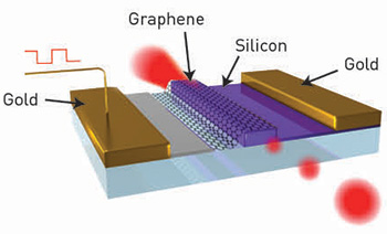 A graphene-based electro-absorption modulator: In a device such as the one demonstrated by Liu et al. in 2011, electrically connected graphene is coupled to a SiO2 waveguide carrying a CW photon stream. [Adapted from M. Liu et al., Nature 474, 64 (2011); reprinted by permission from Macmillan Publishers Ltd., © 2011.]
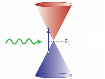 Undoped graphene modulator OFF: For the modulator’s OFF state, under zero applied bias, the Fermi level is at the Dirac point, and graphene is strongly absorbing. [Palash Bharadwaj]
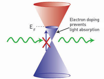 Undoped graphene modulator ON: Under a bias, the graphene becomes electron-doped, and no empty states remain in the valence band for photoexcited electrons, so the device becomes transparent to photons. [Palash Bharadwaj]
Electro-absorption modulators
An ideal EAM should have very fast, tunable absorption for high temporal bandwidth, and broadband operation for high spectral bandwidth. Graphene’s unique optical properties and extremely high carrier mobility allow for just that.
In principle, in a graphene-based EAM, a voltage control pulse changes the electron concentration (and, hence, the Fermi level) in single-layer graphene, causing a strong modulation of its optical absorption. Using these ideas, in 2011, a team at the University of California, Berkeley (USA), fabricated an integrated EAM at telecom wavelengths (λ = 1.55 µm) that operates at speeds up to 1 GHz.
Considering that graphene is just one atom thick, its 2.3 percent absorption is quite remarkable. However, it is not nearly high enough to achieve any meaningful modulation depth in an EAM. The researchers mitigated this problem by coupling the graphene to the evanescent fields of an optical waveguide, thereby boosting the strength of light-matter interaction considerably. Since then, similar devices have been demonstrated that operate at higher frequencies (roughly 10 GHz), an advance made possible by recent fabrication improvements. The speed of these devices is ultimately limited by graphene’s very short photocarrier recombination time (on the order of ps), enabling operating frequencies of hundreds of GHz in principle.
In addition to these applications, graphene also exhibits broadband saturable absorption for moderate optical intensities. This makes graphene a useful material to achieve mode-locking in fiber lasers. Its high nonlinearities also have enabled efficient wave mixing and the demonstration of negative refraction.
Photodetectors and photovoltaics
Graphene’s properties also allow for very fast photodetection—that is, conversion of incident photons to electrical signals. Photodetectors from 2-D materials can utilize multiple mechanisms. The most straightforward is the photovoltaic effect, whereby a photon is absorbed by a semiconductor to yield an electron-hole pair, which in turn is split either by an intrinsic electric field (for example, a p–n junction), or under the influence of an external voltage. Because conduction in graphene can never be turned completely off, applying a DC bias results in power dissipation even in the off state, and is hence undesirable.
Instead, one can use static electric fields that arise when a metal makes contact with graphene due to the difference in their work functions. Metal-graphene-metal devices based on this simple principle, such as several demonstrated in 2013, have achieved a bandwidth of 20 GHz, and form the fastest class of photodetectors to date, comparable to the best conventional Si or Ge detectors.
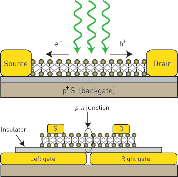 Photodetection and solar-energy harvesting with TMDs: (Top) Photoconductive detector made from MoS2. No appreciable dark current exists in the MoS2 flake owing to its large band gap and low density of thermally excited carriers. Under illumination, the applied source-drain bias separates electrons and holes, resulting in a current almost three orders higher than the dark current. (Bottom) Split-gate p-n junction diode made from WSe2. Biases of opposite polarity, applied to the two bottom split-gates, lead to inhomogeneous electrostatic doping and creation of spatially separated p- and n-doped regions. The resulting p-n junction can be used for photovoltaics as well as light emission.
Another class of hybrid detectors works on the principle of sensitizing graphene with light-absorbing species like organic molecules or colloidal quantum dots. The sensitizer changes its charge configuration upon the absorption of a photon, and effectively “gates” the conduction of electrons in graphene. The striking feature of these detectors is the very high sensitivities that can be achieved. In 2012, a team from ICFO, Spain, demonstrated a sensitivity of 107 A/W, two orders of magnitude higher than the maximum possible sensitivity of an undecorated photovoltaic detector. That boost in sensitivity comes at a price: the bandwidth drops drastically down to about 100 Hz. Even so, such detectors can find use in low-light, video-rate imaging applications, where photons are at a premium but speed requirements are less stringent.
The speed issue becomes still more vexed for photodetectors made from TMDs. Because of their large band gap, TMDs have very few thermally excited carriers, and hence a very small leakage or dark current. The material-dependent band gap offers some degree of spectral selectivity as well. These obvious benefits have triggered a flurry of research activities in this area in the past few years. For example, in 2013, researchers at EPFL, Switzerland, demonstrated an MoS2 photodetector with a sensitivity of 880 A/W; other, similar photodetectors have been demonstrated with WS2 and WSe2.
Yet these state-of-the-art TMD photodetectors can achieve a bandwidth only of a few Hz! This crippling limitation comes from unwarranted “trap” states in these materials, in which charges are held for far too long after the photoexcitation stops. The 2-D nature of TMDs—the property that makes them so exciting—also renders them susceptible, perhaps not surprisingly, to all kinds of perturbations, such as those due to surface charges and chemical contamination. Efforts are currently under way in many labs worldwide to gain a better understanding of these defects, and ultimately to overcome them.
The benefits of TMDs for photodetection carry over to energy-harvesting photovoltaics as well—an area where speed is not critical. Photovoltaic devices aim to produce net electrical energy from photons. That makes it imperative to create doped p- and n-type regions in the same semiconductor, or to use two different semiconductors, one n-doped and other p-doped. In conventional semiconductors, p-doping is achieved by substitutional doping, a strategy that unfortunately has not been perfected for TMDs. Instead, researchers have utilized a clever split-gate geometry to electrostatically dope intrinsic WSe2 into spatially separated electron-doped and hole-doped regions. The resulting p-n junction can be used for photodetection and solar energy harvesting, as was demonstrated in 2014.
Photovoltaic devices can also be fabricated from 2-D heterojunctions. For instance, in 2014, two groups separately reported photodetectors crafted from a heterostructure consisting of p-doped WSe2 and n-doped MoS2. This approach is expected to become standard once large-area flakes with controllable doping can be grown.
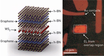 Light emission from TMDs: In a heterostructure of stacked graphene, TMD, and h-BN (left), the graphene acts as electrical contacts, the h-BN as tunnel barriers and the WS2 as the active region, where electron-hole recombination occurs. Such a device, under bias, shows strong electroluminescence from the TMD monolayer (right). F. Withers et al., Nat. Mater. 14, 301 (2015); reprinted by permission from Macmillan Publishers Ltd., © 2015.
Light-emitting devices
Graphene’s absence of a band gap, and, hence, its negligible probability of radiative recombination, makes it a relatively poor candidate material for light generation. On the other hand, TMD monolayers, with their direct band gap in the visible to near IR, are perfectly suited for high-efficiency LED applications, as the direct band gap allows a large radiative recombination rate for excitons. Several groups have recently shown TMD-based LEDs operating under ambient conditions. As with photovoltaic devices, the challenge here lies in defining differently doped regions. Using the split-gate technique, several groups have fabricated LEDs from WSe2 p-n junctions. Another team has seen electroluminescence (EL) from a WS2 device, using ion-gel gating to achieve a similar differential doping and ambipolar transport.
An elegant, qualitatively different LED was fabricated in early 2015 by a group led by scientists at the University of Manchester, U.K. Instead of using a p-n junction, these researchers created a WS2 quantum well by sandwiching it between layers of graphene and h-BN. Electrons and holes injected from the graphene on either side recombine in the WS2, resulting in an EL efficiency of 10 percent, comparable to the best organic LEDs.
Single-photon sources and lasers
The LEDs mentioned above are classical sources, emitting “bunched” photons, and good for applications such as lighting and classical communication. For applications in quantum information, however, one needs a source that generates single photons, one at a time. Such single-photon sources inevitably rely on single quantum emitters such as molecules, quantum dots or defect centers in bulk crystals.
Remarkably, single-photon-emitting defects have been identified in monolayer WSe2 just this year, showing that 2-D materials can generate nonclassical, sub-Poissonian photons. Spatially localized emission from such defect centers shows up at sub-band-gap energies with a very narrow linewidth of about 100 µeV, about two orders of magnitude smaller than the linewidth of the delocalized excitons.
This discovery was reported simultaneously by as many as four independent groups from different parts of the world, attesting to the broad interest and rapid pace of activity in this field. The microscopic origin of the defect is as yet unknown, and so far they are detectable only at low temperatures, but this development bodes well for the future of 2-D materials for quantum optics and quantum information.
A laser represents yet another kind of light source, fundamentally different from thermal or single-photon sources in its statistical properties. It is a perfectly Poissonian (coherent) source: all interphoton arrival times are equally probable. Lasing can be achieved from a gain medium (such as a TMD) by coupling it to a low-loss cavity that provides feedback, and pumping energy into the system externally.
This year, in a first demonstration of a 2-D laser, a team of researchers from the United States, China and Germany has shown narrow-linewidth stimulated emission from a WSe2 monolayer flake by placing it on top of a photonic crystal cavity (PCC). The lasing threshold was very low (roughly 1 W/cm2) in this optically pumped scheme, due to the high quality factor of the cavity (around 10,000) and the large coupling between the WSe2 and the PCC. The device, however, worked only up to temperatures of 160 K, because of increased losses in the GaP PCC at higher temperatures.
Challenges and outlook
Most proof-of-principle 2-D devices thus far have been one-off devices made from individual exfoliated flakes—not a scalable proposition. Any real-world applications will require growth of large-area, defect-free TMD films, similar to what can now be done for graphene. Another pressing challenge is to master control over substitutional doping for TMDs, to obtain well-defined electron- and hole-doped regions in a given material. Chemical doping schemes (ion gels or inorganic molecular adsorbates like AuCl3) and electrostatic doping using split-gates are not really scalable.
Also, as with III-V semiconductors in the past, progress will hinge on improving the quality of grown materials. Even though they are direct-band-gap semiconductors, the photoluminescence quantum yield for most TMD monolayers at room temperature is far less than one percent, almost certainly because of loss channels opened up by impurities and defects in the materials themselves.
For optoelectronic devices, developing a knowledge base of what metals and fabrication processes enable reliable, reproducible electron and hole injection from contacts into TMDs remains a key challenge. The answer may lie in replacing the metal altogether with graphene-based contacts. Whatever the solution, controlling carrier injection is necessary to realize electrically pumped lasers and to further the integration of on-chip electronic and photonic elements.
Graphene has already reached the market in niche applications such as displays. In years to come, TMDs may similarly replace silicon in applications where the latter material’s indirect gap puts it at the greatest disadvantage—that is, in nanoscale lasers and photodetectors. Future work will likely exploit surface modes such as surface phonon polaritons in h-BN and surface plasmons in graphene, and integrate plasmonic optical antennas with 2-D materials. These potential applications, and more, suggest a bright future for optoelectronics in flatland.
The authors gratefully acknowledge funding by the NCCR-QSIT program and the Swiss National Science Foundation (grant 200021 149433).
Palash Bharadwaj and Lukas Novotny are with the Photonics Laboratory, ETH Zurich, 8093 Zurich, Switzerland.
References and Resources
-
M. Liu et al. Nature 474, 64 (2011).
-
G. Konstantatos et al. Nat. Nanotech. 7, 363 (2012).
-
X. Gan et al. Nat. Photon. 7, 883 (2013).
-
H. Harutyunyan et al. Nat. Phys. 9, 423 (2013).
-
O. Lopez-Sanchez et al. Nat. Nanotech. 8, 497 (2013).
-
A. Pospischil et al. Nat. Photon. 7, 892 (2013).
-
B.W.H. Baugher et al. Nat. Nanotech. 9, 262 (2014).
-
R. Cheng et al. Nano Lett. 14, 5590 (2014).
-
S. Jo et al. Nano Lett. 14, 2019 (2014).
-
C.-H. Lee et al. Nat. Nanotech. 9, 676 (2014).
-
J.S. Ross et al. Nat. Nanotech. 9, 268 (2014).
-
C. Chakraborty et al. Nat. Nanotech., doi: 10.1038/nnano.2015.79 (2015).
- A. Srivastava et al. Nat. Nanotech., doi: 10.1038/nnano.2015.60 (2015).
-
F. Withers et al. Nat. Mater. 14, 301 (2015).
-
S. Wu et al. Nature 520, 69 (2015).