
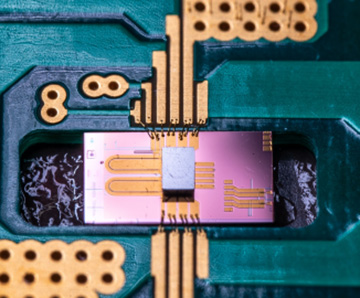
Design of this silicon optical transmitter relied on a “convergence” approach that resulted in a data transmission rate of 100 Gbps—approximately twice that of current state-of-the-art devices. [Image: Photo by Wei Cao, University of Southampton, U.K.]
Ever-expanding internet data centers rely on devices known as optical modulators to help direct the constant flow of electronic data all over the world. But internet traffic and data demands could soon tax their capabilities, a situation driving a search for improved device architectures.
Now, researchers at the University of Southampton in the U.K. report an all-silicon optical transmitter with performance that they say clocks in at around 100 gigabits per second (Gbps)—nearly double the maximum data rate of current state-of-the-art devices made with other materials and processes (Optica, doi: 10.1364/OPTICA.411122).
A convergence approach
The device, says team leader Graham T. Reed, head of the silicon photonics research group at Southampton and an OSA Fellow, is based on a design philosophy that “converges” photonics and electronics into a single integrated system. He says the approach has yielded a high-bandwidth optical transmitter—a modulator plus device driver—that operates at low power and is easily fabricated at low cost using existing chip materials and processes. The team has patented ideas using this design philosophy.
Optical transmitters have conventionally been built by designing the electronic parts—CMOS-based drivers—and the photonic modulators separately and integrating them, Reed explains.
However, Reed continues, “If you use commercial drivers, they tend to be an order of magnitude worse or more in efficiency than our bespoke designs. And normally when you take a modulator and a driver and you combine them, your overall performance is less than the best of the individual parts.”
Better together
Reed says his team’s new approach “put them together and made it better.” He explains that when designing a modulator, you design it for the performance parameters and design of your driver and vice versa. “You design it with the configuration, the performance, the metrics of the particular modulator you want to use it with. The whole thing becomes a mini system design which we refer to as co-design.”
For the new device, the Southampton team, including lead author Ke Li, used a technique called T-coil peaking to increase bandwidth in the CMOS driver/amplifier, for example, which was further enhanced by doping optimization at the silicon modulator junction. Combined, these design choices optimized bandwidth, electrical power efficiency, as well as device footprint, Li says. He expects further improvements as research on the new device and design approach continues.
Future-oriented approaches
Research by other groups to build a better optical modulator includes devices based on thin-film lithium niobate and electronic plasmonics, for example, and some have demonstrated close to 100 Gbps performance, Reed says.
However, he adds, some of these device architectures also require digital signal processing and their novel materials present fabrication challenges like CMOS incompatibility and higher fabrication cost. What is more, he says, the devices typically have not been tested with an integrated device driver, which would drop overall performance and increase power consumption.
But Reed distinguishes between what might be thought of as more future-oriented research with payoffs not immediately knowable and work that merges the advantages of photonic circuits that can be overlayed onto low-cost, easy-to-manufacture silicon chips and wafers today and still realize huge performance advantages.
“Some people are interested in plasmonic modulators,” for example, Reed says. “They tend to be very tiny and that means you could get lots of them onto a fabrication process and costs go down. But it’s not that today.”
Applications beyond data centers
Reed says because of its greatly enhanced performance, the new all-silicon optical transmitter could have applications beyond short-hop connections in data centers. He says the device could be useful in lidar for autonomous vehicles, in 5G telecommunications networks that need short information relays in a city or region, and it could find use in rapidly evolving quantum computing and quantum information systems technology.
For now, Reed says, “we think we can go even faster [with the new convergence device-design concept], as well as using different modulation schemes that are even more efficient. There are people who say silicon modulators are reaching their maximum limit. Hopefully, we have demonstrated with this paper that that isn’t true.”