
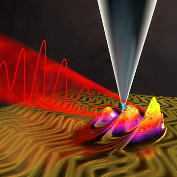
By combining laser pulses (red) with scanning tunneling microscopy, researchers can achieve a temporal resolution of several hundred attoseconds when imaging quantum processes such as an electronic wave packet (colored wave) with atomic spatial resolution. [Image: Christian Hackenberger]
An elusive challenge in the field of microscopy has been to achieve concurrent atomic-scale resolution in both space and time. With a groundbreaking proof-of-concept study, researchers in Germany have demonstrated a new technique that attains this goal by combining scanning tunneling microscopy with ultrashort laser pulses (Science, doi: 10.1126/science.aaz1098).
Such an ultrafast, high-definition microscope has wide-ranging applications in areas like nanoelectronics, lightwave electronics, chemistry and quantum computing.
Bottleneck in the field
Current imaging techniques that are able to resolve objects at the atomic level—for instance, scanning tunneling microscopy—lack the temporal resolution necessary to track electron movement. Ultrafast laser spectroscopy can measure electron dynamics at natural time scales but misses the mark in terms of spatial definition.
For his doctoral work, Manish Garg of the Max Planck Institute for Solid State Research in Germany studied femtosecond physics and found himself becoming frustrated with the low spatial resolution of the technique. As a result, he began working with electron pulses but hit a wall when trying to compress them to shorter time scales, since electrons repel each other even in a vacuum.
“There are a lot of techniques where you have one resolution—temporal or spatial—and you push to get to get the other,” said Garg. “This has been quite a challenge and a big bottleneck in the field.”
Ultrashort optical pulses
Garg and his colleague Klaus Kern, an expert in scanning tunneling microscopy, overcame this obstacle by integrating a phase-locking train of ultrafast laser pulses with a scanning tunneling microscope. For the first time, a technique was able to simultaneously probe electron dynamics in the sub-angstrom and sub-femtosecond regimes, which are the natural length and time scales of atoms.
The researchers focused optical pulses with a time duration of less than 6 femtoseconds into the apex of a nanotip in a scanning tunneling microscope junction. The pulses are precisely tuned with the same carrier-envelope phase, which creates a high electric field that lowers the tunneling barrier. Electrons tunnel between the nanotip and the sample, and by measuring the changes in intensity of this induced tunneling current, they can distinguish atomic-level dynamics in the surface at high speeds.
Garg and Kern demonstrated the power of their device by studying the carrier decay dynamics of collective oscillations of electrons in a gold nanorod.
A camera for the quantum world
This type of optical field-driven tunneling microscopy enables topography mapping of surfaces at the same spatial resolution as a conventional scanning tunneling microscope. The added capability to control electron tunneling at small time scales essentially transforms the microscope into a high-speed camera for the quantum world.
“All electronics are shrinking to smaller dimensions,” said Garg, “and if you want to understand the electron dynamics happening in the small dimensions of a circuit, you should be able to do it with our technique.”