
![]()
An artist’s rendering of the OPERA team’s electrically pumped organic semiconductor laser. [Image: Center for Organic Photonics and Electronics Research, Kyushu University]
A research team at the Center for Organic Photonics and Electronics Research (OPERA), Kyushu University, Japan, has demonstrated an architecture for an electrically pumped organic semiconductor laser diode—a long-standing goal of organic optoelectronics, according to the team (Appl. Phys. Express, doi: 10.7567/1882-0786/ab1b90). The researchers believe that the technology, once matured, could form the basis for a variety of “novel applications” in spectroscopy, displays, biomedicine and visible-light communications (“LiFi”). And several team members have launched a startup firm to develop and commercialize the platform.
The “holy grail”: Electrical pumping
When one thinks of organic optoelectronics—in which the light-emitting layer uses carbon-based, organic materials rather than inorganic semiconductors—the mind goes first to organic LEDs (OLEDs). These devices have seen spectacular progress in recent years, and are becoming commonplace in smartphone and larger displays, lighting and other applications (see “The Age of OLED Displays,” OPN, November 2017). Optically pumped organic semiconductor lasers have also moved ahead smartly in the past two decades, driven by advances in materials and device design.
Bringing organic semiconductor lasers to full potential, however, will require a laser diode that can be electrically rather than optically pumped—and thus that can fully and easily integrated into optoelectronic circuits. And here, the path has been rougher. That’s partly because of significant optical losses at electrical contacts, and severe nonradiative losses in the material as the current densities are jacked up to compensate. The result has been breakdown of the semiconductor material at current levels well below those at which lasing can be achieved.
Building the stack
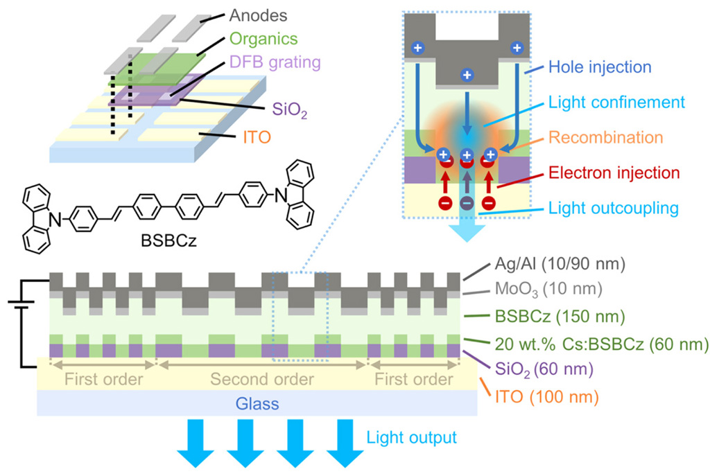
Schematic diagram of the BSBCz-based organic semiconductor laser design and operation. [Image: A.S.D. Sandanayaka et al., Appl. Phys. Express, doi: 10.7567/1882-0786/ab1b90 (2019); CC-BY 4.0] [Enlarge image]
To get around these difficulties, the OPERA team began by focusing on a specific, particularly promising organic material, 4,4'-bis[(N-carbazole)styryl]biphenyl (BSBCz), which is known to sport both good optical properties and the ability to stand up to high current densities. The researchers then built up a stacked structure atop a glass substrate, including a layer of indium tin oxide (ITO) to act as the electron injector, a sputter-deposited and etched layer of silicon dioxide distributed-feedback (DFB) gratings, several BSBCz organic layers for recombination and light confinement, and an MoO3 layer to act as the device’s hole injector. Topping off the structure was an array of silver/gold anodes.
The secret sauce of the device (in addition to the BSBCz organic material) lay in the DFB gratings, the spacing and depth of which were carefully designed to maximize the potential for lasing while reducing optical losses at the electrical contacts. “By optimizing these grids,” the team leader, Chihaya Adachi, said in a press release accompanying the research, “we could not only obtain the desired optical properties, but also control the flow of electricity in the devices and minimize the amount of electricity required to observe lasing from the organic thin film.” The team also doped a thin bottom layer of the organic material with cesium to improve the electron injection into the organic from the ITO layer.
Blue light, lasing signature
In tests of the devices with the DFB grating against reference devices without the gratings, the electrically pumped grating devices emitted blue light with a number of signatures of lasing, including narrow-linewidth emission, a clear lasing threshold and strong polarization. In another sign of lasing, the output was highly sensitive to the cavity geometry—a property that the researchers confirmed by testing multiple devices with different DFB grating architectures.
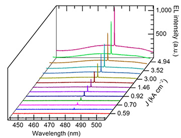
The emission spectra of the organic semiconductor laser (collected in the direction normal to the substrate plane) for different injected current densities. The emitted laser light was collected with an optical fiber connected to a multichannel spectrometer. [Image: A.S.D. Sandanayaka et al., Appl. Phys. Express, doi: 10.7567/1882-0786/ab1b90 (2019); CC-BY 4.0]
While the reference devices without the gratings did show steady-state photoluminescence, they did not exhibit these lasing signatures. That indicated that the grating structure had indeed made the difference and enabled electrically pumped lasing in the organic semiconductor stack.
The team now plans a number of paths toward improving the devices. One research thread to be followed lies in tuning the DFB structure and geometry to further optimize the relationship between the electrical current density and the lasing quality. Other improvements will focus on the materials front; because “the low losses in BSBCz are integral to enabling lasing,” the authors write in the paper, “the development of strategies to design laser molecules with similar or improved properties is an important next step.”
The researchers conclude that the work “opens up opportunities in organic photonics,” and could serve as the foundation for a development of “simple, cheap, and tunable” organic semiconductor laser diodes that can be directly integrated into optoelectronic devices. To help drive forward the commercial development of the technology, several of the study’s authors have launched a startup company, Kyushu Organic Laser Technology (KOALA Tech) Inc.