
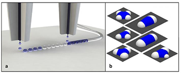
Swiss researchers developed a two-step inkjet printing technique that can make optical waveguides. First, a series of droplets called pinning caps are printed (white); liquid bridges between the pinning caps are then formed by ink deposited in the second print (a). The pinning caps immobilize the ink and prevent the formation of bulges in the printed line. In addition to making straight lines between two dots, the technique can be used to connect three or more junctions to make corners or sharp edges (b). [Image: Fabian Lütolf / CSEM]
Scientists at a Swiss laboratory have demonstrated an inkjet method for precise printing of tiny optical components such as waveguides (Opt. Express, doi:10.1364/OE.26.011934). The new technique leverages capillary forces—instead of fighting them—to make smoother printed lines than previous strategies for inkjet fabrication.
Continuous channels
Photolithography and reactive-ion etching are the established methods for making low-loss optical components on chips, but the resulting structures tend to be fragile. Non-contact technologies such as inkjet printing work for electronic circuitry, but they have been less successful in optics and microfluidics. Such applications require continuous channels—and, at the scale of drops from an inkjet nozzle, surface tension can make even a simple straight line bead up into separate spheroids.
The team at the Swiss Center for Electronics and Microtechnology (CSEM) overcame that problem with a two-step process that actually takes advantage of this property of fluids. The first pass of the inkjet nozzle over a substrate (cladded with magnesium fluoride) deposits discrete acrylic-polymer droplets that the scientists dubbed “pinning caps.” The second pass creates tiny bridges between the caps. The caps don't need to be in a straight line; three or more caps can be joined to form corners and angles, which can eventually form more complex structures.
“The most important step was actually having the idea of using pinning caps to use capillary forces to our advantage instead of fighting them,” says Fabian Lütolf, a member of the research team at the CSEM lab in Muttenz. The scientists had been dissatisfied with the formation of bulges and other issues with previous attempts to inkjet-print waveguides. “Once the capillary bridge idea was born, things came together quickly. We benefited from our past experience, as we already knew how to tune surface energies and had suitable materials and processes at the ready.”
Measuring loss
The CSEM team measured the losses in their tapered optical waveguides at roughly 0.61 dB/cm, with the best single structure registering a loss of 0.19 dB/cm. Although these losses are higher than the 0.02 dB/cm figure that can be achieved with the best lithography, the CSEM researchers say that this is the first time that losses have even been measured in a nozzle-printed waveguide.
According to the team, this additive printing technique could help build complex integrated structures—electronic, optical and microfluidic—on fragile substrates. With this is mind, the team is working toward several practical goals.
“We hope to industrially establish the process for creating multimode waveguides and especially optical interconnects,” Lütolf says. “Besides, we are also looking into different topics like, for example, printed freeform optics, where the printing method could allow novel lens designs in the mesoscale.”