
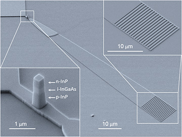
 Scanning electron microscope image showing the fabricated device before metallization. Insets: detail of nanopillar LED (bottom left) and of grating coupler (top right) used to extract the light from the chip.
While almost all long-haul data transmission is optical, traffic within computer systems and microchips is still electronic—and increasingly represents a bottleneck. These connections account for most of the energy consumed by chips. Optical connections, which in principle should be more energy efficient, are obvious successors,1 and numerous research groups are working on enabling these photonic interconnects.
Crucial to tackling this paradigm shift is a light source that can rapidly convert data into light signals, that is small enough to fit into microchip structures, and that scores well in speed and efficiency. Efficiency constitutes a particular challenge, as small light sources, powered by nanowatts or microwatts, have performed very inefficiently to date. Furthermore, the source needs to be compatible with waveguide coupling and integration on a silicon substrate—and while silicon forms the basic material for microchips, it is not a suitable material for light sources.
This year, we demonstrated a waveguide-coupled nanopillar metal-cavity light-emitting diode (LED) that could prove a strong candidate for future optical interconnects.2 Our nano-LED is integrated into a silicon substrate on a membrane of indium phosphide, a suitable material for creating light sources. The nanoscale source is coupled to a low-loss waveguide to enable the routing of light signals and scalability of channel density. Our experiments have shown that the device converts electrical signals rapidly into optical signals and can handle data speeds of a few gigabits per second.
Our work suggests that this integrated nano-LED is a thousand times more efficient than the best variants developed elsewhere.3 The on-chip external quantum efficiency of the new device currently lies between 0.01 and 1 percent at 300 K and 9.5 K, respectively, corresponding to waveguide-coupled power levels of around 22 nW and 300 nW. Furthermore, recent work in our research groups, reporting record ultralow surface recombination velocities of some 260 cm/s in InGaAs/InP undoped nanopillars, reveals that the nano-LED efficiency could be further increased using improved passivation methods.4
Additional developments will be required to improve the device performance and to increase the maturity of the production technology so that it can be exploited by industry. As those improvements come, however, we believe that our nano-LED could offer a promising solution for coping with the future growth of on-chip data traffic.
Researchers
V. Dolores-Calzadilla, B. Romeira, M.K. Smit and A. Fiore, Eindhoven University of Technology, Eindhoven, The Netherlands
References
1. D.A.B. Miller. Appl. Opt. 49, 59 (2010).
2. V. Dolores-Calzadilla et al. Nat. Commun. 8, 14323 (2017).
3. K.C.Y. Huang et al. Nat. Photon. 8, 244 (2014).
4. A. Higuera-Rodriguez et al. Nano Lett. 17, 2627 (2017).