
![]()
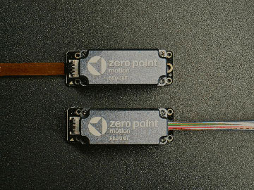
Lia Li. [Image: Zero Point Motion]
The July/August 2025 issue of Optics & Photonics News featured the magazine’s biennial feature spotlighting 10 Entrepreneurs to Watch. Here, we offer an interview with one of those entrepreneurs, Lia Li, CEO of Zero Point Motion. Zero Point Motion develops photonic inertial sensors leveraging semiconductor and MEMS technology to perform in environments that lack GPS.
Can you tell us about what the company is doing and where you’re hoping to take it?
At Zero Point Motion, we’re redefining semiconductor sensors by using light to push the boundaries of detection, and we’re starting with inertial sensors. These are the unsung heroes that allow us to navigate, stabilize and track position—they measure acceleration and rate of rotation, and we’re making them an order of magnitude more precise and stable than what’s on the market today. I think what’s exciting is, we’re not stopping there. We’ve got this roadmap where we can continuously evolve our platform, for example, to include more quantum features, and that allows us to constantly redefine what’s measurable to fundamental limits.
What does that roadmap look like?
Our sensing uses photons, the fundamental building blocks of light, to detect phonons, the fundamental building blocks of motion. We can do this classically, which keeps the cost down and allows us to release our first products sooner and to the widest range of customers. Through high-volume, low-cost semiconductor fabrication methods—the same kind of equipment and techniques used to make computer chips, we can create thousands at the same time on a single wafer. Because you’re making these tiny silicon structures, both mechanical and optical, on the same chip, the photons and phonons are so close together that they’re really deeply intertwined, and that’s where we’re getting this massive boost in sensitivity.
When we think about moving this from the classical to the quantum domain, what we’re doing is engineering the interaction strengths between light and motion to be so strong that we start dealing with single photons and single phonons. We’re really playing on the coupling between light and motion. It’s a fantastic field called optomechanics, and lots of other researchers use optomechanics to detect gravitational-waves or probe the interface between quantum mechanics and gravity.
In our case, we found a neat way to take classical optomechanics and push it into a really high-volume, scalable semiconductor supply chain. But we came out of the quantum research area, so we’re always thinking about how we can bring in more quantum features by just engineering a little bit more, both on the light side and on the mechanical side.
Will those products be fabricated in existing semiconductor fabs?
One of the reasons I focused in on classical sensors when I started Zero Point Motion was because I could see that the existing supply chain was ripe to be able to bring together these two areas, and it’s great to be the first to sit on that intersection. You’re going to discover many new things, and your team is going to be able to tease out so many new concepts and new features. There’s already a market with huge pain points in navigation, especially when global navigation satellite systems are unavailable, jammed or weakened. Customers will be happy with a classical device that’s 10 to 100 times better than what is out there today, and they want it now. So that’s an immediate pull.
We see many quantum computing companies putting great effort and money to mature the supply chains they need in order to create and maintain quantum states; new materials for semiconductors, super low noise light sources, even the electronics. They will pave the way and mature those elements so that we can start to add quantum features to our devices later.
So we have our first product, but then later on, our lives will have been made a little bit easier for quantum because other people have put in the effort to bring up the supply chain. I think especially as a UK company, I was aware that it’s very difficult to grow a deep tech hardware startup. You need huge amounts of capital to generate the supply chain to make that more possible.
For us, it’s all about volume, so scaling and entering large volume markets is our target. But once you’ve tackled scaling, and you see the supply chain is more mature, that’s where we can become quite powerful in pushing quantum into high volumes. Quantum computers, you’re not going to have one on your desk, that’s not the purpose of that market. But you definitely want sensors everywhere and in everything. So we like to think that we’re the underdogs of quantum, and we’ll be able to bring it out into the high-volume markets. We’ll just wait a little bit.
How did you get interested in science broadly, and motion sensing more specifically?
Both my parents are mechanical engineers; they worked in the aerospace industry designing materials for airplane wings. They used to take me into the university when they were doing their Ph.D.s and I would just sit there in the lab and play with all the components and machines and things, so my childhood was kind of spent in an academic environment—specifically in laboratories. I’ve always felt really comfortable in that space, even the smell of the lab is comforting. It was something that really resonated with me, so I always knew that I wanted to do science. I first became interested in particle physics because the Higgs Boson was not discovered at that point, and there was all of this feverish build up to it. When I was 16, I forced my parents to take me to Geneva so we could visit CERN, which was the weirdest holiday request ever from a teenager.
But once you’ve tackled scaling, and you see the supply chain is more mature, that’s where we can become quite powerful in pushing quantum into high volumes.
But when I was doing my physics degree at Imperial College, I realized that particle physics is a lot of intense data processing and coding, and coding isn’t really my favorite thing. I decided that the day-to-day of doing particle physics maybe wasn’t for me. Then while doing my master’s, I built diode-pumped, solid-state lasers from scratch. I’d picked up the project not because I knew I wanted to become a laser physicist, but because I knew I liked tabletop experiments and working with my hands.
And I think that was the first time that I really felt at home in terms of knowing what I want to do every day. To put together some optical components with my own hands, optimize how they interact and then, have the magic moment where a laser beam forms. Ever since then, I knew that I would work with lasers for the rest of my life; there’s something intimate about making it come alive. And lasers are like the best tool ever made. They’re used in every subject matter. When I did my Ph.D., I used lasers to force things to move, to stop them moving, and then to measure them moving. So that’s when motion sensing came into play.
How did you get from there to Zero Point Motion?
I worked in industry for a time, and I was trained to work in a clean room and make MEMS inertial sensors, so that’s how I became familiar with semiconductor sensors. I was really interested in making chips, but I knew it was expensive because you needed a fab, so I kind of pushed that to the back of my mind and stuck with laser physics.
I did my Ph.D. in optical sensing, quantum sensing, using lasers to detect and manipulate motion. And this was an exciting moment in optomechanics, it was before LIGO had discovered gravitational waves. So once again, I was caught up in this moment where everyone’s so excited, everyone’s doing something really different. It’s at the cutting edge. I loved that research, and it was really interesting.
I was really lucky because the University of Southampton opened up their cleanroom to make photonic integrated circuits via their facility CORNERSTONE, and I thought, that’s really interesting, it reminds me of my industry background. I did a few tape-outs with them, and that’s honestly what put it all together. I was like, “oh cool—I get this. It’s chips, photonics, and I can combine this with MEMS—it’s like optomechanics with a semiconductor twist to it.” Everything seemed to slot together so that all the weird things I did in my life added up to something that felt quite meaningful, and I just couldn’t ignore it.
I was really torn about whether to stay in academia; I’d had a few fellowships at that point, and people told me to stick with it and get another one. But I had this really exciting idea that fit so nicely with my experiences, and I really believed there was a market for it. And wouldn’t it be cool to be the person that brings up the team and the company that then becomes the first to ever do this? So I started Zero Point Motion.
Can you talk about the Eclipse and Horizon products?
Eclipse is our market entry, 6-degree-of-freedom inertial measurement unit. It’s not something you’d put in a smartphone; it’s going to be slightly bigger and have a lot more off-the-shelf components. The lasers, detectors—they’re all chip scale, but we’re buying them from other suppliers. We’re not trying to make them in our semiconductor fabrication process. We knew there were markets that were desperate for better performing industrial sensors, mainly for things like safety and autonomy. In mining and construction in particular, you don’t have a stable GPS signal. You’re often indoors or underground. And you can’t install beacons everywhere, you can’t just put cameras everywhere, but you do want to know precisely where your digger head is. You don’t want to hit any infrastructure lines. And often you don’t want people to be the eyes and ears of monitoring that. You want to do this as autonomously as possible.

Our Horizon product, on the other hand, is the big play. We take the Eclipse but now the lasers, detectors, all the electronics—it's all made together on the same chip. That brings down the cost and the size, for use in drones, phones, cars, AR/VR, smart appliances, robotics. That’s the exciting future, where we’re bringing a level of precision that has so far only been accessible to aerospace or defense.
Why did you decide to bring more integration and packaging R&D in house?
I’m a first-time founder, and our team walks a fine line between two separate semiconductor industries—no one has been on this path before. When we started out, we decided to use various companies and suppliers, but what you don’t realize is, you’re a tiny startup, and nine out of 10 startups fail. So you’re not the priority for big companies or suppliers. And at our scale, every day we’re losing money if we don’t have the product out, whereas bigger companies can wait longer.
Our decision to bring integration and packaging in-house was really born out of the pain of experiencing delays with no leverage to push back. It’s a global supply chain, so even something like supplies being held in customs for a week was a real killer for us. It was like, oh my gosh, how can we even iterate—your first pancake never turns our right, you know? I was very lucky that my lead hardware engineer, Sergejs, is not just visionary but he’ll grind day and night to make things happen. He said he could do it in-house, and he set up our lab so we can perform our own wafer probing, laser integration, detector integration, bonding, metrology, packaging, everything. And we’ve reduced something that would take eight weeks down to a day.
Is it a production factory floor? No! We’re doing maybe 20 or 30 devices quickly because we just want to learn. We want to know soon as possible about any design flaws or issues. Now, a really good question is, have we done things in our lab that are better than existing methods when it comes to creating and assembly sensors? That’s potentially an opportunity that can be explored in the future, which would be exciting for the UK, to increase presence in the semiconductor supply chain. For now, we are just happy that we get to cut down the time scales.
Are there key lessons that you’ve learned as part of this process?
As an entrepreneur, you learn fast because you have to! Startups run on speed and curiosity. If you’re not learning every day, you’re not building fast enough.
I think one lesson is to enjoy the messiness of innovation. It’s scrappy to get from the lab to a product. You have to be aware that there are unknowns, not just in the science itself, but unknowns about who you are, what you can do, what your team can do, what the limits are. You get some of those elements right, and you suddenly realize it’s such an exponential boost in what you can achieve by yourself.
I have to remind myself every day to try and enjoy that process because even if things don’t go the right way, what you’ve gained in terms of knowledge, belief in yourself and other people, and understanding of how the world works is infinitely insightful. It builds even more creativity and curiosity.
In photonics, one of our biggest opportunities but also challenges is that it’s such a broad landscape. You can do anything with photonics, any research you want, but it’s not naturally embedded in our research framework to think about an end product. These outcomes aren’t as well defined like they are for some fields in engineering. So how do you bring that discipline to a research area that is so naturally academic, and less industrial in the sense of reaching consumer markets?
What is your longer-term vision for the technology?
I talked about the quantum side, and that comes from a desire to push the boundaries and bring as much cutting-edge science into what we’re doing as we can. But the other vision is to think about the bigger picture of sensing.
We realized that we’re at the intersection between two existing supply chains. When we tried to model ourselves as a pure MEMS company or a pure photonics company, it never worked because we’re in the middle. So we’ve got to create our own rule book and our own way of thinking. Then when we started bringing stuff in-house, we realized that we were really creating a platform architecture—it’s an entirely new way to think about making sensors that we built from the ground up. When we get to Horizon, we’ll have solved all the bottlenecks in bringing photonics into the consumer market.
Then we looked around, and we thought, “Oh, you could do this for optical microphones, ultrasound sensors, clocks, RF MEMS—any semiconductor device could be optically enhanced.” The next wave of compute, sensing and interconnect is going to be done by photons, by the fabric of light. Every sensor we make, the data are encoded in light first and foremost, and it could fuel AI, manufacturing and autonomy.
So if I was to really tell you my big passion project, I think it’s this idea of redefining every single type of sensor that we currently use and having light embedded into them.
When I think about why I would want to work at Zero Point Motion had I not founded the company, it’s that vision of changing the way sensors were designed in the past and doing it a different way. Light is the enabler, and suddenly you don’t have to play the same rules as you did before. And I think that’s what would make me, if I wasn’t the founder of the company, join a scrappy startup.
Our values are really simple—passion, integrity and focus. The focus is we have a core product, inertial sensors, and we know that really well. But we’re also really passionate about the big picture—changing how sensors are created. The integrity is how we communicate and make decisions. We’re really honest about what’s going right, what’s going wrong. We hold ourselves accountable; if someone else can’t do something for us, we’ll do it ourselves because we’re so determined.
I think all of that means you’ve got to be working toward a vision. Because if we just stopped at one sensor, yeah, it might be a really cool company, but startups are really difficult, and it’s grunt work a lot of the time. You need something that’s fueling the team to get past the difficult bits to reach an almost unobtainable but hugely transformation step change in technology. That’s the motivation and the vision.
