
![]()
A NIST trapped-ion chip. [Image: Daniel Slichter, NIST/OSA Quantum 2.0 Conference]
The opening keynote talk of OSA’s new Quantum 2.0 meeting, delivered by Marissa Giustina of Google AI Quantum, focused on the development of Google’s widely discussed quantum computer. That machine, dubbed Sycamore, was built on a platform that used superconducting circuits as quantum bits, or qubits.
But such circuits constitute only one possible platform for quantum computing. A lively follow-on session at the all-online conference on Monday looked at some of the remarkable developments afoot in some alternative platforms, such as trapped ions and atoms—as well as elsewhere in the superconducting-circuits game.
Exploring trapped ions
Daniel Slichter of the U.S. National Institute of Standards and Technology (NIST) started things off with a look at NIST’s efforts to push trapped-ion quantum processors to new levels of integration and compactness. These qubits differ from the superconducting qubits in Google’s machine, he explained; instead, they involve arrays of ions that are laser cooled and optically pumped in ultra-high vacuum, with the quantum state read out from the energy level of the trapped ion. The platform has some advantages, Slichter noted: trapped ions are identical, tend to have long coherence times, and offer high-fidelity control.
Integrating trapped-ion processors on a chip-scale platform, however, is tricky and an ongoing project at NIST. Part of that project involves reconfiguring the RF traps (Paul traps) that the institute uses for ion confinement—a quadrapole setup involving two RF rods and two DC rods—into a flat design that can be made not macroscopically in a machine shop, but on a chip using standard microfabrication techniques.
Another piece of the puzzle, Slichter said, could lie in developing what he called a “quantum CCD architecture,” in which ions are moved between different zones on a chip, such as a “gate zone,” a “memory zone,” and a “readout zone,” to execute different parts of the computation.
Toward an integrated trapped-ion unit cell
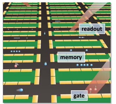
In his Quantum 2.0 talk, Daniel Slichter sketched out a suggested “CCD architecture,” in which trapped ions would be moved as needed to different functional zones on the chip. [Image: Daniel Slichter, NIST/OSA Quantum 2.0 Conference]
Getting to that point will require “integrating more control into the trap itself,” according to Slichter. Among the ways to do this might be using current-carrying nanowires on the chip to use magnetic fields to control qubits in a “laser-free gate.” Another might be integrating photon detectors right in the trap to read the fluorescence signal, rather than relying on external detectors.
At the end, Slichter sketched out an ultimate vision, and yet-to-be-realized goal, of a “unit cell” in a trapped-ion chip that would include a data ion carrying the quantum information; a “helper” ion that could function both to sympathetically cool the data ion and provide a fluorescence channel for reading out its data; an integrated photon detector to actually measure the fluorescence; electrode nanowires to create magnetic-field gradients; and integrated laser beams to control the helper ions. “There are no external components you have to align,” he said. “You plug some fibers and electrical wires in the chip, and it runs.”
Penning traps
Later in the day, another speaker from NIST, John Bollinger, took the audience through an alternative approach to trapped ions: large “ion crystals” controlled in a Penning trap, which uses static magnetic and electric fields to confine charged particles. While he admitted that RF traps, such as the Paul traps that Slichter discussed, have been “the workhorse for trapped-ion processing,” Bollinger noted that Penning traps are “a proven system for forming and controlling” such crystals, and even allow the amassing of 3D crystals of more than 105 ions.
In working with these systems, NIST uses lasers to cool Be+ ions for trapping and prepare quantum states, and reads out the signal via fluorescence. The platform has been useful in quantum simulation, sensing and entanglement experiments at NIST. Bollinger suggested that it could also find use in noisy intermediate-scale quantum (NISQ) processing, through a system of programmable single-site ion rotations that NIST is working on.
From ions to atoms
Benjamin Bloom, the co-founder of the start-up Atom Computing, looked at a different system, programmable arrays of trapped neutral atoms—which he jokingly referred to as “the ugly cousin of trapped ions.” Neutral atoms, he admitted, are very hard to trap, but “that makes them very good qubits.” Indeed, he pointed out that coherence times of more than 10 seconds have been demonstrated, and that substantial progress has been made in capabilities to re-arrange atom arrays on the fly; in low-atom-loss imaging from the arrays; and especially in large-scale entanglement of neutral atoms.
Bloom said he co-founded Atom Computing with Jonathan King in 2018 with the near-term aim of building “an externally accessible programmable neutral-atom NISQ computer.” His organization has focused on alkaline earth elements—especially 87Sr—for which cooling techniques have improved dramatically in recent years, and which offer some advantages, particularly in a wide menu of quantum states to play with.
The company uses optical tweezers—laser beams focused through a microscope objective—to trap and manipulate atoms; indeed, by shining multiple beams through the same objective, it’s possible to create a holographic array of traps. Bloom even showed an “atom Etch-a-Sketch,” tracking out the company’s logo by moving a single confined atom. The company’s efforts are now focused on scaling the system to more complex arrays.
Tweezer clocks and quantum sensors
Adam Kaufman of JILA/University of Colorado has also been working on atomic arrays of ultracold 87Sr, controlled via optical tweezers—particularly for use in metrology and many-body physics experiments. Tweezers offer “a simple yet powerful platform,” he said—and while he didn’t focus specifically on quantum computing in his talk, he stressed that the numerous other applications that the platform has enabled “highlight that getting to scalable quantum computing with tweezers is a promising endeavor.”
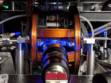
A photo of JILA’s neutral-atom trapping setup. [Image: Adam Kaufman, JILA/OSA Quantum 2.0 Conference]
The interest in 87Sr as a platform stems, Kaufman said, from the diversity of transitions that the two valence electrons of the element allow, which open up the prospect of doing a variety of different things, including imaging, ground-state laser cooling, and clock functions/optical frequency metrology. Indeed, the JILA team recently unveiled a new “tweezer clock” architecture by combining these degrees of freedom.
Looking ahead, his team hopes to build on that foundation to combine the versatility of optical tweezers (for functions such as generating entanglement) with atomic clocks, and thereby create long-lived entanglement in programmable quantum sensors.
Superconducting qubits redux
One other talk in the session, by Jerry Chow of the IBM T.J. Watson Research Center, took the focus back to the superconducting-qubit platform described in the meeting’s keynote. IBM has concentrated its own efforts on this platform, unveiling what Chow called the “first quantum computer in the cloud” four years ago. That effort has since expanded, Chow says, to include some 256,000 registered users that have run more than 400 billion quantum circuits and produced more than 400 scientific papers.
“We are in an interesting spot now,” Chow noted. “How do we grow this community?” He cited three requirements for that: quantum systems that push the envelope; access to cloud-based open-source resources for algorithm development (such as IBM’s own Qiskit); and what Chow called “quantum enablement”—developing the quantum workforce and professional services needed to grow the market. “The enablement piece is really the biggest piece,” he said. “That’s what’s really going to drive progress for this industry.”
The (long) road from NISQ to fault-tolerance
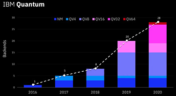
Chow noted that, in its superconducting-qubit machines, IBM had made substantial progress in “quantum volume”— defined as the “largest computational space a device can explore.” [Image: J. Chow, IBM/OSA Quantum 2.0 Conference]
One thing that Chow suggested is that, under the circuit model, “a classical computer is really just a very poor quantum computer”—the unit of computation is still the circuit. The near-term problem is how to develop circuits that run on quantum hardware, and programming them to do things that classical computers can’t do. Chow walked through some of IBM’s efforts to attack those problems on multiple fronts, including the use of the concept of “quantum volume”—the “largest computational space a device can explore”—as a metric for gauging progress.
The long-term challenge, Chow said, is moving beyond NISQ machines to actual fault-tolerant universal quantum computers. That’s a problem that has a long time horizon. The steps toward that goal, Chow suggested, lay in fully exploring the NISQ space and using it to lay out a path toward developing true quantum applications. “There’s a lot of room to continue to grow,” he concluded.