
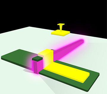
A U.S. team has designed a structure for an electrically powered nanoscale-LED—consisting of a 160-nm-wide ZnO fin (purple), a metal electrode (yellow), a thin layer of isolating dielectric (dark green) and a GaN base (light green)—that reportedly produces light 100 to 1,000 times brighter than other LEDs of comparable size, and that lases at a sufficiently high driving current. [Image: NIST]
Wide-band-gap semiconductor light-emitting diodes (LEDs) have been among the most successful of photonic technologies, revolutionizing general illumination, display, sensing and other applications. As with everything else, researchers continue to seek ways to make these devices ever smaller, to drive new nano-applications. But electrically pumped nanoscale LEDs have an Achilles’ heel: “efficiency droop,” the tendency of the LEDs’ quantum efficiency to fall off when the current density pumping them exceeds a certain threshold. This droopy behavior has thus far limited the power outputs of nanoscale LEDs to nanowatts or less.
Now, a multi-institution U.S. research team reports a tiny LED that seems to get around these limitations (Sci. Adv., doi: 10.1126/sciadv.aba4346). The new device, based on a p-n hetrojunction featuring slender fins of zinc oxide, reportedly continues to gain brightness as more current is pumped in, sidestepping efficiency droop. And, even more surprising, if you pump enough power into the structure, it turns into a tiny laser—with no conventional laser cavity.
The team says that its sub-micrometer-area LED can generate light 100 to 1,000 times brighter than conventional LEDs of comparable size, reaching the tens of microwatts. While the design thus far has been reported only in the near-UV, the researchers believe that it can be extended to other wavelengths as well, giving it potential in chip-scale applications in sensing, displays, disinfection and more.
The droop conundrum
Efficiency droop actually is a feature of all LED technologies; indeed, it’s one reason that lighting manufacturers are increasingly looking at lasers as alternatives for certain general-illumination applications (see “Lighting with Lasers,” OPN, July/August 2020). The droop problem becomes especially acute, however, as LEDs are shrunk to micrometer or sub-micrometer scales, where it can limit power outputs to picowatts or nanowatts.
The causes of efficiency droop—defined as a decrease in the LED’s internal quantum efficiency (IQE) with increasing current density—remain an object of some debate. Researchers have uncovered possible links to nonradiative recombination, stimulated emission, leakage currents and other effects. Making matters worse, there’s also a related “temperature droop,” with IQE decreasing still more as the junction temperature increases due to the higher current density.
A finny solution
The research team behind the new work—including scientists at the U.S. National Institute of Standards and Technology (NIST), the University of Maryland, Rensselaer Polytechnic Institute, and the IBM T.J. Watson Research Center—apparently weren’t seeking a solution to droop, but only a new architecture for shrinking down LEDs for use in chip-based applications. To do so, they experimented with a design very different from conventional planar LEDs.
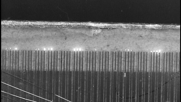
The team fabricated comb-like arrays of the fin-based LEDs; some of them are shown emitting in this micrograph. [Image: NIST] [Enlarge image]
The team’s design begins with a p-layer of gallium nitride (GaN) that serves as a base for the device. On top of that base, the researchers epitaxially lay down a thin “fin” or filament of zinc oxide (ZnO), the n-layer, roughly 5 µm in length and around 160 nm wide. A thin layer of dielectric material is laid down on either side of the fin, and a metal electrode, to feed in the driving current, completes the LED assembly. Each fin so constructed forms a single LED pixel; the team also combined these pixels into arrays of submicron-scale LEDs in a comb-like structure.
From LED to laser
In a press release accompanying the research, lead author Babak Nikoobakht, who conceived the design, noted that he “thought that [the fins’] elongated shape and large side facets might be able to receive more electrical current.” To find out, he and the team started pumping current into the structure, with an eye toward seeing how much it could take before it burned out. To the researchers’ surprise, the structure just kept emitting brighter and brighter light (in near-UV wavelengths) as the driving electrical current increased, emitting at powers two to three orders of magnitude higher than conventional LEDs of similar size.
As the team pushed the device to still higher driving currents, another surprise was in store. At current densities higher than 500 kA/cm2, the device’s relatively broad-spectrum emission (centered at 385 nm) narrowed into two tight, intense lines of 403 and 417 nm. In other words, at sufficiently high current densities, the LED—far from suffering from efficiency droop—actually becomes a laser diode. The ZnO fin, under the right conditions, appeared to be acting as a Fabry-Pérot cavity.
To get to the bottom of this unusual behavior, the team dug in with some numerical modeling. The team’s modeling suggested that the fin architecture mitigates two specific kinds of nonradiative (that is, non-light-producing) electron–hole recombination in the semiconductor—Shockley-Read-Hall (SRH) recombination and Auger recombination. These mechanisms are thought to penalize photon production in conventional LEDs, and have been previously implicated as possible culprits in efficiency droop.
Small and bright
The absence of efficiency droop and the lasing behavior in particular, Nikoobakht suggested in the press release, gives the team’s device “a lot of potential for being an important building block” in various photonic applications. These could include chip-scale applications in sensing, handheld communications, displays and even disinfection. And the team believes that the study just published lays the groundwork for “further reduction in cavity size below sub-100 nm,” potentially opening additional application spaces.
“While it isn’t the smallest laser people have made,” said Nikoobakht, “it’s a very bright one.”