
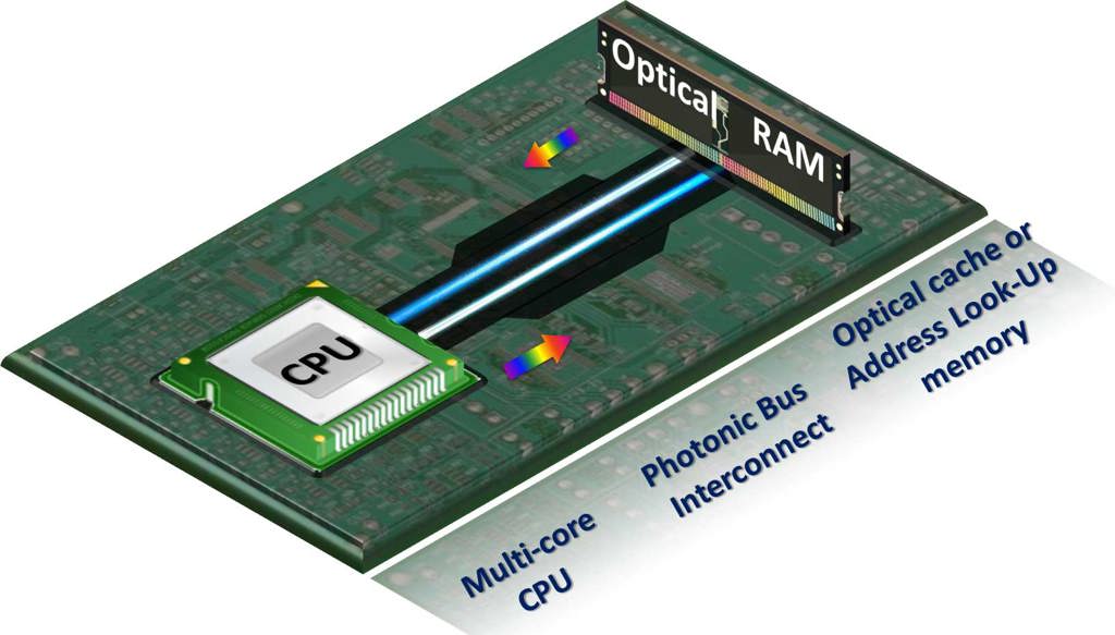
An artist’s rendering of the Aristotle University team’s proof-of-concept optical RAM, separated from the CPU by an optical interconnect. [Image: Courtesy of C. Vagionas] [Enlarge image]
The computer industry is now thoroughly preoccupied with trying to extend the benefits of Moore’s law, which has allowed processor power to grow exponentially for decades but which appears now to be running up against its limits. But another fundamental issue has long bedeviled computer engineers: a “memory wall” that has caused the speed of chip-based random-access memory (RAM) to grow at rates far slower than computer CPU speeds. The memory wall imposes a built-in bottleneck that slows down aspects of CPU-memory interchange such as data buffering and lookup operations—a bottleneck that will only become more troublesome in an era of big data and high-bandwidth communications.
Now, a research team from the Aristotle University of Thessaloniki, Greece, believes it has come up with an architecture that can break through the memory wall. And the team’s solution rests squarely on optics.
In work published last month (Opt. Lett., doi: 10.1364/OL.44.001821), the team demonstrated an all-optical RAM cell architecture that reportedly can double the speeds of electronic RAMs. And although the team’s proof-of-concept device currently has a larger footprint and higher per-bit energy consumption than electronic alternatives, the researchers believe that some materials and photonic-integration engineering can address those shortcomings.
Divergent growth

Christos Vagionas at CLEO 2019, San Jose, Calif., USA.
The new study’s corresponding author, senior researcher Christos Vagionas—who will present the work this afternoon at a session on high-speed optical interconnects at the 2019 CLEO Conference in San Jose, Calif., USA—explains that memory speeds have recently grown at rates of only around 7 percent annually, compared with the still-rapid 52 percent annual growth in electronic CPU clock speeds. Those divergent rates have opened an increasing speed gap between processor and memory.
“Each time you wanted to reach out and fetch data from memory that was off chip,” says Vagionas, “you had to face this memory wall bottleneck.” He adds that, with fiber optic line rates now coming in at 400 gigabits per second, and with rates greater than a terabit per second on the roadmap, the memory wall could start to become a real problem in settings such as high-performance routers, where the destination addresses for data packets will need to be looked up within the line rate to keep things humming along.
Beyond the flip-flop
Since the late 1990s, numerous research groups have attempted to use optics to scale the memory wall, with some “very nice demonstrations,” according to Vagionas. But many of those demos have been simple one-cell “flip-flop” storage architectures, rather than fully functional RAM that supports read operations, write operations, and access control. And the optical RAMs that have been demonstrated have tended to max out at rates of 5 Gbit/s, comparable to electronic memories.
One reason for the speed ceiling for optical memory, according to the researchers, is that the architecture of systems demonstrated thus far has tended to mimic electronics. Electronic RAM uses two separate lines to control access to a memory cell: one for the bit signal, and one for its inverse, the bit (“bit-bar”) signal. That means two sparate access gates to control the two bit streams.
Vagionas’ team wanted to see if they could get to higher speeds by taking advantage of the optical wavelength dimension. In the team’s device, the inverse signals are generated at two different wavelengths—λ1 for bit and λ2 for bit-bar—and sent through a single channel, with random access controlled through a fast optical push-pull gate. “This allows us,” Vagionas says, “to transmit them at the same time and effectively look like a single CW with constant power, over the same ‘wire,’ or photon waveguide.”
Doubling RAM speed
The team’s proof-of-concept device consists of a single optical RAM cell that includes a semiconductor optical amplifier Mach-Zehnder interferometer (SOA-MZI) serving as an access gate. That gate is tied, via an arrayed waveguide grating (AWG), to an indium-phosphide set-reset optical flip-flop unit.
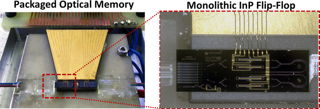
A photo of the Aristotle University team’s device. [Image: Courtesy of C. Vagionas]
In tests of the unit, the team was able to demonstrate all core RAM operations—read, write and random-access—at rates of some 10 Gbit/s. That’s twice the rate of other optical RAM demonstrations and electronic RAMs, according to Vagionas.
Reducing energy costs
Right now, the team sees the biggest potential for the new device in the top end of the market—high-performance computers, and high-end routers that will be under industry pressure to boost address lookup rates as communications line rates continue to increase. But over time, Vagionas says, the chip could find other uses, such as speeding up pseudo-random binary sequence (PRBS) generators for testing and encryption.
While the device seems to have a clear speed advantage and to open an opportunity to get past the memory wall, it also has a few shortcomings. One is its relatively large footprint—12 mm2, versus the square-micron or smaller chip acreage of other memory demos. And the Aristotle University team’s RAM also is a bit of an energy hog, requiring 200 pJ/bit, versus fJ/bit-scale energy consumption for slower RAM cell demos.
Vagionas notes that the energy disadvantage may not be as large an issue as it seems in some configurations where a CPU is communicating with distant RAM that lies off-chip. That’s because electronic-to-optical conversion itself imposes a memory cost on the order of 100 pJ/bit. Keeping the memory in the all-optical domain could eliminate the need for such conversion going into and out of the memory.
Nonetheless, Vagionas says the group is “fully aware that optical memories have to start being comparable with electronics” in terms of footprint and energy costs. He believes that this will be possible by replacing the semiconductor optical amplifiers on the chip—chosen for the demo owing to their track record of robustness and reliability—with integrated-photonic technologies and materials such as photonic crystals and phase-change memories. These techniques, on which the group is currently working, could, according to Vagionas, hammer down footprint and power consumption to levels of a few square micrometers and a few fJ per bit.
“Each first step,” Vagionas says, “has to rely on stable operation—it’s too complicated to proceed in both ways. You proceed one step by developing a new technology, and then you scale it down for better performance.”