
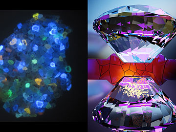
At left, natural diamonds glow under ultraviolet light owing to their various nitrogen–vacancy (NV) centers. At right, a schematic depicting the diamond anvils in action, with NV centers in the bottom anvil. [Image: Norman Yao, Berkeley Lab; Ella Marushchenko]
Most conventional sensors aren’t made to withstand the enormous temperatures and pressures that occur near the center of the Earth. And many are not small enough to fit into the tiny region where these conditions are created in the laboratory.
Now, researchers based at two U.S. labs have harnessed atomic-scale impurities in diamond anvil cells to measure the magnetic and stress fields of metals under high pressures and temperatures (Science, doi:10.1126/science.aaw4352). The technique pinpoints the locations of features in the fields instead of averaging them over the entire sample.
Tiny cells, extreme conditions
Diamond anvil cells, developed six decades ago, consist of two diamonds with small flattened points, called culets, that face each other. These gems are, of course, the hardest known substance, and virtually incompressible themselves, and the culets are only a couple of hundred microns wide. When they push down on a sample in a cell filled with a compressible fluid or gas, the anvils create a minuscule region of extreme pressure and temperature—hundreds of gigapascals (GPa) and thousands of Kelvins (See “Photonic Eyes on Earth,” OPN, July/August 2019).
The scientists at Lawrence Berkeley National Laboratory and the University of California, Berkeley, tweaked the anvils by seeding them with a layer of diamond nitrogen–vacancy (NV) centers about 50 nm from the surfaces of the culets. These atomic-scale impurities—in which a carbon atom in the diamond lattice is replaced by a nitrogen atom and a lattice vacancy—have electronic spin ground states that are highly sensitive to nearby changes in stress, temperature and electromagnetic fields.
The researchers detected the conditions these NV centers were experiencing by scanning them with 532-nm-wavelength laser light focused to a diffraction-limited spot roughly 600 nm wide. A scanning confocal microscope picked up the fluorescent signals from the defects and created a 2D map of the conditions across the culets.
![]()
Co-lead authors Satcher Hsieh (left) and Chong Zu tune the laser of their imaging system. [Image: Marilyn Sargent, Berkeley Lab]
Under pressure
The team measured the magnetization of iron as the intense pressure surrounding it drove a phase change from one type of crystal structure to another. Backing off the pressure slightly to chart a hysteresis loop demonstrated that the critical pressure for the phase change is roughly 13.6 GPa.
Next, the scientists investigated the pressure–temperature diagram of gadolinium, a rare-earth element, under high pressures but cryogenic conditions as low as 25 K. Gadolinium behaves quite differently from iron under these conditions—for example, its P-T diagram doesn’t lead to a neat hysteresis loop.
Toward other exotic materials
The authors propose that their technique could be modified for different experiments—say, by introducing silicon–vacancy centers, rather than nitrogen–vacancy centers, in the diamond anvils. Other hard materials, such as moissanite (silicon carbide), could host atomic defects that could serve as sensors in experiments that require larger anvils than diamonds. Ultimately, the team hopes that their technique will lead to new explorations of superconducting hydrides and other exotic materials.
Researchers from Iowa State University, USA, Carnegie Institution of Washington and Ames Laboratory, USA, and Ludwig-Maximilian-Universität, Germany, also contributed to the study.