
Photo of array of lasers on silicon, mounted on copper heat sink with gold wire bond connections. [Image: Courtesy of Alwyn Seeds, University College London]
Scientists at three U.K. universities report that they’ve developed a technique to grow electrically pumped, telecom-wavelength lasers directly on silicon—a step that they label “a major advance” toward practical silicon-based photonic-electronic integration (Nat. Photon., doi: 10.1038/nphoton.2016.21). The technique, which combines the use of quantum dots (QDs) for laser gain with some novel process tweaks to minimize power-sapping material defects in the gain layer, reportedly allows the fashioning of continuous-wave InAs/GaAs lasers directly on a silicon substrate, with high reliability and with an extrapolated laser mean time to failure of more than 100,000 hours.
Lattice mismatch
Growing lasers on silicon is a long-sought goal—but it’s been tough to realize practical light sources directly in silicon, owing to the material’s indirect band gap. To get around that limitation, much of the work on silicon-based light sources has thus focused on using wafer bonding to join direct-band-gap group III-V semiconductor laser materials, such as gallium arsenide and indium phosphate, to silicon substrates.
Growing the III-V lasers directly on the silicon, through standard techniques such as molecular beam epitaxy, is in principle more attractive and less costly than wafer bonding for large-scale production. Unfortunately, lattice mismatches between III-V materials and silicon lead to the formation of “threading dislocations,” tiny defects in the crystal structure that can play havoc with laser gain—particularly for the quantum well lasers that have been a focus of much recent research.
Radiative recombination
“If you’re trying to make a laser, you want radiative recombination,” explains Alwyn Seeds of University College London (UCL). “If you’ve got a dislocation, what you’ll end up with is most of the current being used up in non-radiative recombination.” And, he adds, the dislocations can also drastically reduce effective device lifetimes—a shortcoming that, he says, has undermined previous efforts to grow quantum well lasers on silicon.
One way to get around the lattice mismatch problem has been to deposit an intermediate layer of germanium between the silicon and the active layer. But germanium absorbs light at typical telecommunications wavelengths of around 1,300 nm, making it a poor choice for that part of the spectrum.
Quantum dots and dislocation filters
Seeds—along with UCL colleague Huiyun Liu, other UCL scientists, and researchers at the University of Sheffield and Cardiff University—decided to attack the lattice-mismatch problem head on, using two tactics. One was to use thin gallium arsenide films with nanocrystalline quantum dots, rather than quantum well structures, for laser gain. QDs are less sensitive to the impact of threading dislocations and other defects, as they are distributed, localized point sources of light—which means that a given threading dislocation can only quench the emission from a small number of QDs, leaving the rest unaffected.
The other tactic was to minimize the density of the threading dislocations themselves, through some adjustments in the epitaxial growth processes. Liu and several other team members developed techniques including changes in annealing times; a 6-nm-thick “nucleation layer” of AlAs between the silicon and the III-V layers, to absorb much of the effect of the lattice mismatch; and a superstructure of four GaAs layers atop the nucleation layer, separated by “dislocation filter layers” that guide the path of threading dislocations in a lateral direction and cause them to annihilate one another.
The result is a layered structure of GaAs in which the density of threading dislocations falls off dramatically only a micrometer or so away from the silicon interface (see image). For the active QD layer at the top of the structure, the dislocation density is only around 105 per cm2—roughly an order of magnitude less than the typical value for GaAs on silicon, and a practical value for a QD laser. “At 105 dislocations, a quantum well laser is still in trouble,” says Liu. “For quantum dots, it’s no problem at all.”
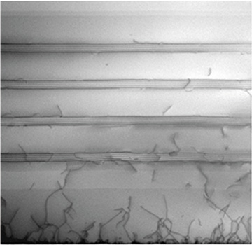
The density of threading dislocations (linear features) falls off dramatically with distance from the silicon interface (bottom), in part owing to a structure of thin “dislocation filter” layers separating 300-nm-thick GaAs layers. Area shown is approximately 3,000 nm2. [Image: Courtesy of Huiyun Liu, University College London]
Long laser lifetimes
According to the team, the lasers that result from the method, operating at a wavelength of 1,310 nm, have some promising characteristics, especially for communications applications: room-temperature output power of 105 mW, operation to 120 °C, and an extrapolated mean time to failure of more than 100,000 hours.
The last parameter, says Seeds, is particularly important, as previous demonstrations, whether using quantum wells or quantum dots with a germanium layer, have topped out at extrapolated lifetimes of 4,000 hours or less. “For equipment used in optical or data communications, you would want lifetimes in excess of 40,000 hours,” he notes. “Otherwise it’s never going to be a product.” The technique also reportedly boasts a high yield of working lasers, another variable of keen interest to manufacturers. “We get lots of lasers,” says Liu, “and almost 100 percent work.”
The next steps for the team will be, according to Seeds, looking at “the standard laser development issues,” and how to use the technique to push forward integration of optics and electronics on a single platform. “It might take a little while,” says Liu, “but that’s the final goal we’re tied into—to solve the silicon photonics problem.”