
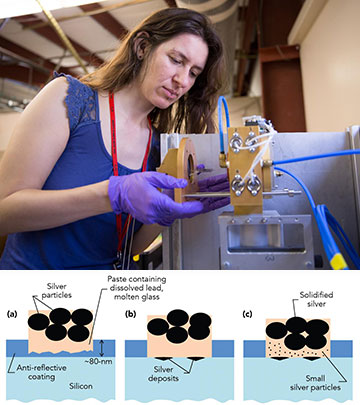
(Top) Vanessa L. Pool, a postdoctoral researcher at SLAC's Stanford Synchrotron Radiation Lightsource, with the experimental apparatus. (Bottom) The experiments revealed in detail how steadily increasing heat results in the formation of silver solar-cell contacts with three layers: silver particles at the top (left), silver deposits in the pitted silicon surface (center), and an intermediate glass-silver layer between (right). [Images: SLAC National Accelerator Laboratory]
A team of U.S. scientists has leveraged X-ray imaging to get a clearer view on a narrow but important problem in photovoltaics: precisely how the microns-thin, expensive silver electrical contacts on conventional silicon solar cells form during manufacture (Nat. Commun., doi: 10.1038/ncomms11143). According to the researchers, the insights gained could help in the search for cheaper—and more environmentally friendly—ways to make solar cells.
Getting the lead (and silver) out
Notwithstanding the advent of alternative materials such as perovskite, silicon solar cells still own more than 90 percent of the market. The electrical contacts on a majority of those silicon cells are made of thin grids of silver, using a process known as screen printing—essentially deposting a paste of silver and a glass “frit” consisting of silica and lead oxide onto the surface of the cell, and then firing the combination at some 800 °C for less than a minute. The result, when the cell has cooled, is a grid of 50-micron-wide silver lines etched into the silicon surface.
Surprisingly, although screen printing has been used for decades in manufacturing photovoltaics, no one has known precisely how contact formation actually works, chemically and mechanically, in the extreme conditions of the furnace. That’s important, because manufacturers would like to find substitutes for costly silver in fashioning the contacts (one of the most expensive solar-cell components), and also to dig up more environmentally friendly alternatives for the lead used in current production.
X-ray vision
To get a better look at how these contact forms, scientists at the U.S. Department of Energy’s National Renewable Energy Laboratory (NREL) and the SLAC National Accelerator Laboratory turned to X-rays to illuminate the process. The team started by building a small-scale industrial furnace at the SLAC Stanford Synchrotron Radiation Light Source. Then, they ran sample solar cells through the furnace and used the synchrotron source to fire X-rays at the sample as it heated, obtaining diffraction data at 250-ms intervals, to allow for a granular view of the structural and chemical changes taking place during the firing process.
The team found that the formation of the silver grid takes place in three stages: melting of the glass-lead frit at above 500 °C, which wets the interface between the silver and silicon; reaction of the lead oxide and the solar-cell’s anti-reflection coating at between 500 °C and 650 °C, which etches the cell surface and gives the silver channels in which to pool; and dissolution and diffusion of the silver in the frit above 650 °C, followed by a redox reaction that ultimately leads to the deposition of metallic silver on the emitter surface.
The contact resulting from the process consists of three layers: solid silver on top, a thin glass intermediate layer impregnated with silver crystals, and metallic silver in pits etched into the silicon surface.
Looking toward alternatives
The research team believes that understanding the process in this new level of detail could help illuminate potential alternatives to both costly silver and toxic lead in the production process. In particular, given the intricate chemical interdependence of the silver, silica and lead during the cell’s time in the furnace, alternatives to both the silver and the lead in the screen-printed paste need to be developed at the same time, to ensure the right mutual solubility, reactivity, and transport kinetics throughout the process.
In that quest for alternatives, the researchers add, the new process they’ve developed to track how the contacts form could prove quite handy—replacing a before-and-after, “black box” view with continuous, real-time observations of the process. “This tool,” says Maikel van Hest of NREL, “will have a great impact in the photovoltaic industry, as well as in basic research.”