
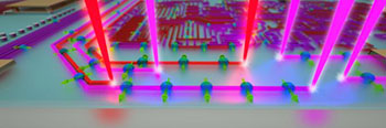
Artist’s conception of using light beams of different wavelengths to fashion quantum circuit elements on a topological insulator. [Image: Peter Allen]
Taking advantage of a serendipitous discovery, scientists from three U.S. universities have demonstrated a technique that uses fine beams of light to create persistent yet reversible circuit elements on the surfaces of the materials known as topological insulators (Sci. Adv., doi: 10.1126/sciadv.1500640). The researchers believe that the approach could not only provide new inroads for studying the exotic physics of topological insulators, but could help the materials realize some of their potential applications.
Since their experimental discovery 2008, topological insulators—materials that, by virtue of their topological order, behave as insulators in bulk but as conductors on their surfaces and edges—have attracted attention, as their spin-polarized surface states and symmetry characteristics hold promise for applications in spintronics and quantum computing. But there’s been a hitch: Chemical methods for fabricating logic gates on the materials, as well as approaches such as doping that are standard in semiconductor manufacture, can, by messing with the material’s topological order, destroy the very properties that make topological insulators interesting in the first place.
Accidental discovery
Recently, scientists from the University of Chicago stumbled upon a possible alternative route to writing circuits on topological insulators. They found that turning on the lab’s fluorescent lights led to “a slow drift in our mesurements” of a thin film they were studying for a different purpose, according to grad student Andrew Yeats, the lead author on the study. The Chicago scientists, along with colleagues at Pennsylvania State University, soon established that the material’s substrate, SrTiO3 was responding to a particular wavelength in the fluorescent lighting—and that the effect could be harnessed to create an optical stylus to change the chemical potential of local areas on the film without adding other materials or violating its topological order.
Specifically, the experiments involved a thin film of (Bi,Sb)2Te3—the topological insulator in the system—atop the SrTiO3 substrate. Shining light of the right wavelength onto the material modulates a space-charge layer in the substrate, which induces a persistent field effect that locally changes the chemical potential in the overlying film. It’s analogous to what would be accomplished with electrostatic gating, but it’s done entirely optically, with no added materials and no chemical processing. The sign of the effect, too, depends on the wavelength (and thus the energy) of the illumination, which makes the effect optically reversible.
Light-written transistor elements
Via this technique, the scientists were able to pattern onto the film a p-n junction, a key transistor element, by using red light to initialize an area as p-type, and then using UV light to gate certain rectangular subregions as n-type. To test whether the process had harmed the topological-insulator properties of the film, they measured the materials in high magnetic fields to check for a property called weak antilocalization, known to be associated with the surface-state transport characteristics of these materials. They found the expected signatures in the optically gated material, which suggested that its unique surface states had indeed survived the optical tweaking.
Other tests, meanwhile, indicated that the optical gating persisted for some 16 hours without significant relaxation. That persistence, as well as the fact that the optical gating can be erased and rewritten “in less than a second,” according to team leader David Awschalom of Chicago, suggests its potential as “a platform for optically defined reconfigurable electronics.”