
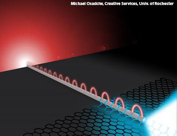
Wire plasmons propogate to the distal end where they interact with 2-D semiconductor MoS2 flake.
Researchers from the United States and Sweden are using a new material combination to meld electronic and photonic devices into one circuit. This new integrated nanophotonic circuit design could lead to computer chips that deliver information at the speed of light (Optica, doi:10.1364/OPTICA.1.000149).
The team, made up of scientists from the University of Rochester and the Swiss Federal Institute of Technology in Zurich, created a “primitive” nanophotonic integrated circuit from a silver nanowire and a single-layer molybdenum disulfide (MoS2) flake. The use of MoS2 flake as a seminconductor is a break from the traditional hybrid nanophotonic circuits that use graphene. MoS2 trumps graphene in this application because of its potential use as both a transistor and a photodetector.
To test their new combination, the researchers used a laser to excite plasmons on the exposed surface of the silver nanowire. Using a scanning confocal fluorescence microscopy and spectroscopy, they observed that the MoS2 flake at the far end of the circuit photoluminesced in response to the excited plasmons propagating down the length of the wire. They also observed that the decaying excitons from the MoS2 light were re-collected as nanowire plasmons. The ability of their prototype to preserve signal intensity—the shuttling of light back and forth between the MoS2 flake and exposed end of silver nanowire—holds promise for transmitting information in very small dimensions via nanophotonic integrated circuits.
Although photonic devices can transmit information faster than electronic devices, they are often bigger because their components cannot be miniaturized like electronic circuits. However, 2-D materials like graphene and MoS2 flake offer interesting photonic properties with very little bulk. For example, as MoS2 flake becomes thinner, the transfer of energy between electrons and photons becomes more efficient.
In the paper, the authors state that their design’s potential for subwavelength light guiding and strong nanoscale light-matter interaction may allow for compact and efficient on-chip optical processing. Next, the team wants to create a near-field detector based on MoS2, as well as MoS2 LEDs coupled to on-chip nanoplasmonic circuits.