
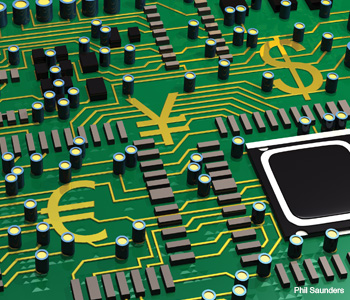
The field of silicon photonics is at a unique inflection point: Paths for commercialization are now widely accessible, and the costs and risks associated with prototyping products have dropped precipitously. Building optical devices with the same silicon processing tools and wafers that the semiconductor industry uses to fabricate CMOS transistors gives us access to an immense infrastructure for yield improvement, metrology and process control.
By taking advantage of the high refractive index contrast between silicon and silicon dioxide—and using silicon-on-insulator wafers similar to those employed for advanced transistors—engineers can now construct micrometer-scale integrated optical circuits. This technology holds promise to meet the world’s ever increasing demand for bandwidth, and may open opportunities in a wide range of applications, including medical diagnostics, LIDAR, spectroscopy, radar systems, biosensing and more.
The field of silicon photonics has benefitted from the billions of dollars invested in CMOS fabrication. This established infrastructure allows for a high level of integration: devices that modulate, detect, route and filter light can all be co-located on the same wafer and built using the same tools. This is in contrast to the current state of optical systems, where modulators might be fabricated in lithium niobate, detectors in III-V wafers, optical multiplexers with doped glass and switches with MEMS; everything is typically connected via lenses or optical fibers today.
The downside of leveraging the CMOS infrastructure is the cost of accessing it: Developing a silicon photonics process is at least a multi-million dollar endeavor. Fortunately, it is no longer necessary to start from scratch in most cases. A number of organizations around the world, including the A*STAR Institute of Microelectronics (IME), CEA-Leti, Imec and others, have now developed processes with various levels of capability, and they are offering them to the wider community. Typically, a dedicated run in a process that yields waveguides, high-speed modulators and photodetectors will cost hundreds of thousands of dollars.
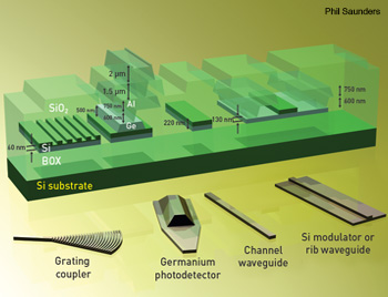 Building blocks of silicon photonic systems.
The benefit of using a pre-existing process is that it largely or completely eliminates process development risk. Multi-project wafer services such as the Optoelectronic Systems Integration in Silicon (OpSIS) service at the University of Delaware and the silicon photonics platform ePIXfab allow users to buy into runs for only a few square millimeters of area.
In addition, there are several processes that can be used to fabricate transistors next to the optical components, such as IBM’s 90-nm CMOS-photonics platform and Luxtera’s and PETRA’s processes, though these are not yet publicly accessible. Much current development is focused on low-capacitance bonding between the standard foundry silicon for electronics and the silicon photonic wafers, since this obviates the need to make technical compromises, as well as the cost disadvantages associated with monolithic integration. Simply put, monolithic integration works well for trailing-edge CMOS, but incorporating high-performance CMOS into such an approach is all but impossible without significant performance compromises.
Bonding processes for electrical interconnects are mature and commercially available, and they provide an elegant solution to electronic-photonic integration, although co-integration of electronics will not be necessary for all applications. Several companies (Skorpios, Aurrion) are now developing platforms that integrate III/V lasers into silicon, but there are not yet any released products based on such processes, and the processes themselves are not yet available to the public.
In the absence of monolithically integrated transistors and optics, there are varying levels of alternative integration schemes available: separate optical and CMOS chips in a 2.5- or 3-dimensional integration scheme; optical and electrical chips placed together on a printed circuit board; a standard form factor; or stand-alone packaged optical devices.
Economies of scale
Silicon photonics has thus far been an expensive industry for startup activity, where the only players were those with immediate access to foundries that were willing to change their process to accommodate optical devices; however, this may be beginning to change. Luxtera and Kotura have produced products in silicon, for example. Multi-project wafer runs in silicon photonics reduce the financial risk of prototyping, while at the same time providing clear paths for scaling to production.
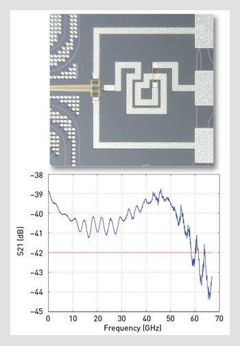 High-speed photodetector. (Top) A high-speed photodetector fabricated in the OpSIS-IME platform with an inductor for gain-peaking bandwidth enhancement. (Bottom) The device has 57 GHz bandwidth.
Just considering modest volumes of tens or hundreds of wafers, it’s clear that the processes used to build silicon photonic systems—including all of the mask and setup costs—drop to the low tens of thousands of dollars per wafer very quickly, and then to thousands of dollars per wafer shortly thereafter. A 200-mm wafer represents around 30,000 usable square millimeters of space. So, for a 10-mm2 product, this can represent thousands of devices. The bottom line is that getting to cost targets of a few dollars per chip does not require producing millions of devices, even for relatively complex chips.
Such opportunities are not limited to active components either; there are myriad interesting passive systems that can be fabricated, for instance, through OpSIS’ shared multi-project wafer runs. In fact, in the 1 March 2010 issue of Optics Express, Fang et al. report a 200-GHz spacing 32-channel AWG fabricated in a similar process at the A*STAR IME with competitive performance to commercial offerings. An off-the-shelf array waveguide grating may be on the order of $1,000 for a 32-port device in small volumes. Even at small-to-medium volumes, silicon can compete with existing products from a cost perspective; in both cases the costs usually end up being dominated by packaging. The big opportunity for silicon photonics is in cramming more complexity—and thus more value—into a single package.
Building blocks of silicon photonics
The financial story becomes more compelling when one considers the systems possibilities enabled by silicon photonics. Typical circuits consist of a few fundamental building blocks built on a silicon-on-insulator wafer: passive components such as waveguides, couplers and filters, and active devices such as modulators and photodetectors. Using these, large systems can be pieced together without significant reengineering at the device level.
Researchers have already extensively demonstrated high-performance devices. Narrow single-mode and wide multimode waveguides can route light around a chip with losses near 2 dB/cm and 0.026 dB/cm, respectively. Mach-Zehnder modulators have been shown to be capable of data rates up to 50 Gbps and rings at rates of up to 40 Gbps. For detection, Vivian et al. present a germanium photodiode at 120 GHz with 0.8 A/W responsivity at 1,550 nm in the 16 January 2012 issue of Optics Express. Although none of the previous devices were built in an integrated platform with modulators and photodetectors, the OpSIS platform does offer 57 GHz, 0.7 A/W photodetectors alongside 30 GHz modulators and other library elements.
Given the advanced state of many devices in silicon, the question arises: Why are there so few demonstrations of very large optical systems? Well, there are several reasons. Barriers to building these types of systems include: immature design tools, a packaging ecosystem that is only beginning to be able to handle silicon, and the relatively high historical expense of doing systems-level work. Still, the greatest advantage of using silicon in photonics, just as in the microelectronics industry, is that we can use it to build complex systems. We’re just beginning to see complex system integration projects emerging. It’s an exciting time in the field.
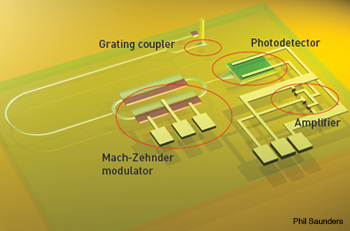 A simple optical link. Link consists of a grating coupler, modulator, detector and amplifier.
Examples of these complex systems in the literature range from phased-array antennas to biosensing to data communication. In the 9 January 2013 issue of Nature, Sun et al. report on a large-scale 2-D optical phased array antenna with 4,096 nano-antennas integrated onto a single chip. They were able to project the MIT logo in a far-field pattern. Doylend et al. demonstrated an integrated on-chip laser with a grating coupler array for beam steering at the 2013 Photonics West conference. And Mandal and colleagues integrated 16 biosensors onto a single chip using 1-D photonic crystal resonators; their results are available in the 4 February 2008 issue of Optics Express.
In the data communication realm, Dong et al. present an integrated 224 Gb/s coherent silicon transceiver with on-chip polarization diversity in the 2013 proceedings of the OFC/NFOEC conference. In the 1 March 2010 issue of Optics Express, Fang et al. report on a 32-channel WDM receiver. Finally, an MIT/Lincoln Labs team demonstrated a packaged photonic ADC to sample a 10-GHz optical signal in the 13 February 2012 Optics Express. As we address the barriers to building complex systems, we can expect silicon photonic systems to rapidly expand in both functionality and complexity.
Quantum silicon photonics
Integrated quantum photonics is one of the applications that may be enabled by more advanced silicon photonic foundry services. (For a general review of integrated quantum optics, see Tanzilli et al. in the references.) By leveraging non-classical properties of light such as entanglement, superposition and uncertainty relations, researchers are developing disruptive technologies. Most notably, quantum cryptography allows for unconditionally secure secret key distribution, while the prospect of a quantum computer that is able to factorize large numbers means that current encryption schemes may become obsolete.
Because of its compatibility with the telecommunication network, silicon photonics is obviously a platform of choice for building economical and practical emitters and receivers for quantum cryptography. To give an overview of the challenges, and to argue for the enabling role of foundry services, we take as an example the ambitious implementation of linear optical quantum computation, the “holy grail” of applied quantum optics.
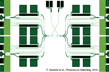 Mask layout of 100 Gbps PDM-DQPSK. System fabricated through the OpSIS shuttle run service.
Knill, Laflamme and Milburn explored how to build a quantum computer that relies on individual photons, their interference and detection in a seminal paper in 2001. The key components that must be assembled together in a scalable circuit are:
-
A source of highly indistinguishable single photons.
-
Probabilistic quantum gates based on beam splitters and phase shifters.
-
Efficient single-photon detectors and feed-forward control of switches.
Are they available in silicon today? Remarkably, the answer is “yes” (including hybrid solutions), although no one has built two of these pieces on the same chip. Thus, the gap between device and system-level work applies equally well to quantum optics. There are several solutions with which to implement these three components:
A source of highly indistinguishable single photons: The nonlinear process of spontaneous four-wave mixing (sFWM) can be used to generate pairs of identical photons from two pump beams symmetrically detuned in energy from the pair. Several groups have now demonstrated correlated photon pair generation using sFWM. (See Ken-ichi et al. in the June 2011 issue of the New Journal of Physics; Azzini et al. in the 8 October 2012 Optics Express; Davanco et al. in the 25 June 2012 Applied Physics Letters; and Matsuda et al. in the 12 November 2012 Scientific Reports.) However, in all cases, the level of integration remains primitive. Indeed, the experiments were mainly performed off-chip, including the filtering and rejection of the pump beam or beams and the manipulation and detection of single photons.
|
Today’s foundry services such as OpSIS and epixfab already offer all the necessary tools to build passive structures for pair generation. Interestingly, though, they offer a clear path to the integration of efficient, tunable wavelength filters to reject the pump beams. The challenge here is to improve the solutions used in traditional wavelength multiplexing applications to achieve extinction ratios above 100 dB due to the vastly greater intensity of the pump compared to the single photons.
Probabilistic quantum gates based on beam splitters and phase shifters: Two-qubit quantum gates have been demonstrated in passive and thermally tunable silica glass waveguides. They require only phase shifters and directional couplers and are therefore straightforward to build and assemble in large circuits through a multi-project wafer run.
Efficient single-photon detectors and feed-forward control of switches: Single-photon detection is arguably the most challenging technological problem that must be solved in silicon quantum photonics. Impressive results have been obtained using hybrid integration of superconducting nanowires evanescently coupled on top of silicon waveguides, with detection efficiencies greater than normal-incidence detectors. Yet it is hard to see how this approach could be scaled to the same level as the silicon photonic circuits. Fortunately, a fully CMOS compatible solution may exist: an avalanche Ge-on-Si photodiode operated in Geiger mode (biased above breakdown), similar to what is used in commercial single photon counters based on silicon (for visible) and III/V materials (for telecom).
Remarkably, the very same components, tools and architectures developed for high-volume classical applications can be transposed with little or no modification to operate in the quantum regime. Of course, some of the figure-of-merits emphasized in classical applications will not be relevant to quantum circuits, such as bandwidth or energy consumption; loss, stability and uniformity will be the key metrics in quantum optics. But with only a slight shift of focus, silicon photonics opens the fascinating perspective of putting the counter intuitive features of quantum mechanics at work at unprecedented scales.
Final hurdles
Shuttle run services such as OpSIS or ePIXfab are mirroring practices well known to the microelectronics industry. Services such as MOSIS have provided researchers across academia and industry the tools and processes to build complex electronic systems at little risk. Aside from the cost savings that shared shuttle runs offer the community, they also provide design rules and well-characterized devices as part of a process design kit. Rather than designing a library of parts from scratch, users can piece together a series of devices that are known to work. However, what is missing from this equation is the electronic design automation infrastructure for design verification.
Before fabricating large integrated electronic systems, an engineer may simulate the chip layout across process corners, compare it to a schematic, and check for layout errors that will not yield in fabrication. Unfortunately, only the design rule checking exists as a somewhat mature toolset for optical design.
Compact models and schematics for verifying the final layout and performance of designs are still in their infancy. There are, however, several promising tools that are beginning to address these issues, such as Mentor Graphics Pyxis and Calibre, Lumerical Interconnect, and the IPKISS component design framework. As more features are added to these tools, the complexity of systems being taped out through multi-project wafer runs will also likely increase. A central challenge for the near term will be in standardizing the model sets and characterization methodologies, but this is now being taken on by industry organizations such as Si2.
Whether they develop complex systems or not, most research groups now have the means to at least bring a silicon photonic product to market. Even in very small volumes, the chip costs of silicon photonic devices rapidly shrink to the point where they will be in the few-dollar range. Other costs, such as packaging and lasers, will often dominate the overall price of silicon photonic solutions. There are already products available from Kotura and Luxtera, and it is likely that even relatively complex photonic circuits will cost hundreds of dollars or less, including packaging costs, without having to go to extremely high volumes. Very complex, low-volume photonic circuits will sell for thousands of dollars or more, with this cost largely driven by the non-recurring engineering associated with their development.
We will see, in the next few years, a boost in the number of silicon photonic products coming to market and an increase in the number of complex silicon photonic systems being developed in academia. Furthermore, novel applications such as chip-scale quantum optics will continue to emerge, creating fundamentally new commercial and research opportunities over the coming years.
The authors would like to thank Mentor Graphics, Lumerical and Gernot Pomrenke of the Air Force Office of Scientific Research for their support of the OpSIS project. They also acknowledge support from Brett Pokines of AFOSR SOARD (FA9550-13-1-0176) and the Singapore MOE under ACRF Tier 1 grant R-263-000-A09-133.
Matthew Streshinsky is a Ph.D. student at Institute of Microelectronics (IME), A*STAR, Singapore and the National University of Singapore (NUS). Michael Hochberg is the director of OpSIS and a professor of computer and electrical engineering at the University of Delaware, U.S.A., and at NUS. Patrick Lo is director of the NanoPhotonics Program at IME. Christophe Galland and Prof. Tom Baehr-Jones are scientists at the University of Delaware and Andy Eu-Jin Lim is a scientist at IME.
References and Resources
-
T. Baehr-Jones et al. Nat. Photon. 6(4), 206–8 (2012).
-
K. Lister. www.luxtera.com/20120221252/luxtera-ships-one-millionth-silicon-cmos-photonics-enabled-10gbit-channel.html (2012).
-
T. Tanzilli et al. Laser Photon. Rev. 6(1) 115–43 (2012).