
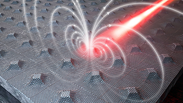
Artist’s rendering of nanopillars in strained graphene, which can give rise to large pseudo-magnetic fields in the material, changing its optical properties. [Image: Courtesy of D. Nam]
Graphene—atomically thin, 2D sheets of carbon, whose discovery captured the 2010 Nobel Prize in physics—has some remarkable properties. It’s strong, yet super-light; it’s hard, yet flexible; and it boasts extremely high electron mobility and a brisk photoelectric response. Thus the material is finding its way into designs for a variety of next-gen optoelectronic devices, in components such as modulators, photodetectors, low-loss waveguides and more.
One possibility, however, has remained elusive. Because graphene is a zero-band-gap material, it’s been hard to find a route to graphene lasers.
Researchers in Singapore have now taken an intriguing step toward that goal, by tweaking the strains in the material’s ultrathin sheets (Nat. Commun., doi: 10.1038/s41467-021-25304-0). Specifically, the team has shown that engineering a periodic structure of nanoscale pillars into a graphene sheet can produce localized tensile strains that give rise to extremely strong pseudo-magnetic fields. Those fields, in turn, can affect electron transport, open up energy gaps and significantly modify the material’s optical transitions. The result, the authors argue, could presage “a new class of graphene-based optoelectronic devices,” including lasers.
Faking magnetic fields
It’s been known for some time that subjecting graphene to an external magnetic field can create energy gaps in the 2D sheets, by affecting charge-carrier motion and relaxation times. The problem has been that pulling off the feat requires rather intense fields—on the order of those produced by laboratory-scale superconducting magnets. That’s hardly a practical approach for creating integrated electronic and photonic devices on the chip scale.
One alternative explored in the past decade has been creating a pseudo-magnetic field within the graphene itself, through judicious strain engineering. A variety of studies have shown that straining graphene flakes at the nanoscale can generate strong localized gauge fields, effectively giving rise to enormous pseudo-magnetic fields—as beefy as 800 T in one recent study. Those fields, in turn, should in principle allow development of so-called Landau quantization (discrete energy levels tied to electron motion in a magnetic field) in the graphene, thereby building an energy-gap structure in an otherwise zero-band-gap material.
Nanopillar array
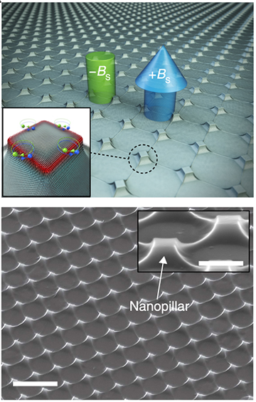
Top: Nonuniform tensile strain at the edges of graphene nanopillars induces pseudomagnetic fields of opposite signs. Bottom: SEM image of nanopillar array (scale bars: 2 µm in main image, 1 µm in inset). [Image: D.-H. Kang et al., Nat. Commun., doi: 10.1038/s41467-021-25304-0 (2021); CC-BY 4.0]
What’s been missing from the picture has been experimental testing of how these giant pseudo-magnetic fields actually affect graphene’s optical properties. To take a step in that direction, the research team led by Donguk Nam at Nanyang Technological University, Singapore drilled down into the dynamics of “hot” charge carriers—electrons and holes—in strained graphene.
To create a platform for the experiments, the team started out with a rectilinear array of nanopillars, chemically etched into an SiO2/Si substrate and then topped with a 20-nm-thick Al2O3 layer. A graphene layer was then wet-transferred onto the top of the nanopillar array, and muscled into conforming to the array topography via capillary forces. Graphene’s exceptional mechanical properties allowed the accumulation of large, localized tensile strains—and, thus, the potential of strong pseudo-magnetic fields—at the nanopillar boundaries.
The team then used scanning electron microscopy and Raman spectroscopy to characterize the strain distribution in detail. Numerical modeling using the measured strain values suggested that the nanopillar-deformed graphene should host pseudo-magnetic fields as high as 100 T near the points of strongest deformation.
Measuring carrier relaxation
Finally, to see how such deformation-induced fields might affect the graphene’s optical properties, the Singapore researchers dug down into the strained graphene’s charge-carrier dynamics. Specifically, they fired femtosecond pump pulses into the material to excite charge carriers, followed by probe pulses at varying delay times to suss out how long it took the carriers to relax down to their original energy level.
The team found that the strained graphene sported carrier-relaxation times more than an order of magnitude longer than in unstrained graphene. Further experiments and numerical modeling suggested that the electron behavior was consistent with the formation of pseudo-Landau levels—and, thus, the creation of an energy-gap structure—in the graphene.
Graphene lasers ahead?
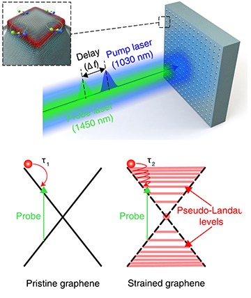
Pump–probe experiments (top) demonstrated a significant deceleration of the relaxation time of charge carriers in strained versus unstrained graphene, consistent with the development of Landau quantization in the material. The behavior could, according to the authors, enable the creation of pseudo-Landau-level lasers and other new optoelectronic devices in graphene. [Image: D.-H. Kang et al., Nat. Commun., doi: 10.1038/s41467-021-25304-0 (2021); CC-BY 4.0]
Team leader Donguk Nam told OPN that under this system, the pseudo-magnetic field “can be easily tuned by varying the size of the nanopillars.” That, he maintains, makes it possible to have “an infinite number of unique graphene devices with different band gaps.”
More intriguing still, Nam says, is the possibility of leveraging these techniques to create graphene-based lasers. In a theoretical study published early this year in Optics Express, the Singapore team argued that Landau quantization due to pseudo-magnetic fields in strained graphene could make the material “an excellent gain medium” that would support the building of chip-scale graphene lasers.
Thus the team’s demonstration and analysis of the optical properties in the strained 2D material should, Nam maintains, help with the project of “realizing the world’s strongest, thinnest lasers.” Such graphene lasers, he says, would “complete the last missing link toward the realization of all-graphene electronic-photonic integrated circuits … which is anticipated to revolutionize the way computer chips work.”
Correction, 31 August 2021: The story has been updated to properly reflect the source of quotations in the last section.