
Researchers designed reconfigurable metasurfaces with 2D spirals that deform when a voltage is applied. Each of the spiral units act as a pixel and can be independently manipulated. The researchers demonstrated the metasurface by using it to create a hologram display. [Image: Jiafang Li, Beijing Institute of Technology] [Enlarge image]
Much of the research on electromagnetic metasurfaces and metamaterials has focused on static configurations. Increasingly, however, scientists and engineers are looking at so-called dynamic metasurfaces, the optical properties of which can be actively reconfigured by applying a voltage, deformation, heat or some other external change (see “Tunable Metasurfaces,” OPN, July/August 2021). Now, a research team in China has designed dynamic, ultrathin, programmable metasurfaces that can control light at the nanoscale level (Opt. Express, doi:10.1364/OE.434321).
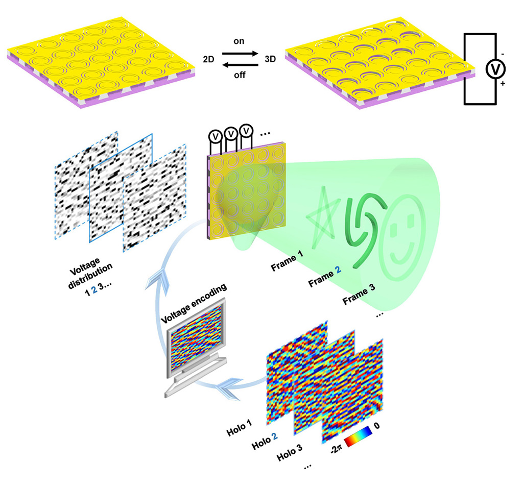
Inspired by the designs in kirigami, a variation of origami that involves both folding and cutting of paperlike surfaces, the scientists at the Beijing Institute of Technology (BIT) developed a thin, patterned gold-over-silicon structure that provides electromagnetic control of individual pixels within the structure. They predict such optical elements could eventually be incorporated into such applications as 3D displays, data storage systems and digital light projectors.
From art to chip
According to the BIT researchers, led by physicist Jiafang Li, the arts of origami and kirigami have served as models for other types of 3D microstructures and nanostructures based on materials such as graphene and polymer. Some of these devices employ pneumatic or mechanical means of deforming these metasurfaces, but true electromagnetic control of individual pixels has remained challenging.
First, Li and his BIT colleagues created a thin, nanopatterned film. Each unit cell in the tiny pattern consisted of two Archimedian spirals, with the cells spaced 2 μm apart. The researchers used electron-beam lithography, ion-beam etching and wet etching to carve the 2D spiral pattern into a 60-nm-thick gold film.
The team suspended the gold film over a silicon substrate with 400-nm-high silicon dioxide pillars separating the two layers. Applying a voltage to the device deformed the spiral pixels by a maximum out-of-plane height of 230 nm.
Proof of concept
To test the device, the BIT scientists used it in two different types of scenarios. First, they produced a holographic design—an image of a spiral-type windmill—by applying a single voltage to the device. Second, they applied different levels of voltage to individual pixels of the lattice and generated designs of a smiley face and five-pointed star in addition to the windmill.
The BIT team noted that its proof-of-concept experiment had a grid of only 32×32 pixels. More would be needed to increase image detail. Also, according to the researchers, combining the reconfigurable metasurface with the same type of multi-line addressing method employed in some organic LED (OLED) displays could improve the device’s ability to control light.