
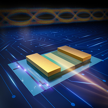
Artist’s rendering of III–V photodetector fabricated on authors’ InP/SOI platform. [Image: Hong Kong University of Science and Technology]
A team of Hong Kong–based engineers has demonstrated what it believes is an improved technique for growing high-performance photodetectors made from III–V materials directly on a platform compatible with silicon photonics (Optica, doi: 10.1364/OPTICA.431357). The team’s approach cleverly puts together several micropatterning and deposition techniques to create a monolithic indium-phosphate/silicon-on-insulator (InP/SOI) platform tuned for growing such devices in a variety of dimensions.
The researchers believe that their approach skirts some of the shortcomings in current methods for building photodetectors for photonic integrated circuits (PICs) on silicon. As a result, it could, the team writes, point to “a practical solution for the monolithic integration of III–V active components and Si-based passive devices on an InP/SOI platform in the future.”
Stringent performance requirements
As data communications and data traffic have continued to grow, seemingly without limit, optical interconnects using silicon photonics have emerged as a cost- and energy-efficient approach to replace increasingly overstressed and power-hungry data-center electronic links. In that quest, fast, high-performance photodetectors obviously constitute a key element.
To operate effectively in the interconnect game, such integrated photodetectors need to sport a demanding combination of characteristics. These include large bandwidth, operation across a broad wavelength band, high responsivity (the efficiency with which the photodetector converts light into electrical current), and low “dark current” (background current in the absence of incident light). But they also need to play well with the existing CMOS manufacturing system—and, in particular, to couple efficiently with optical waveguides on silicon.
Partial solutions
As the authors of the new study observe, several material systems have stepped up to try to meet these requirements on silicon. One is germanium-based materials, which are generally compatible with silicon and sport a large bandwidth and good responsivity at telecom wavelengths. Nonetheless, these materials, the authors say, are prone to lattice mismatches that create crystal defects, or dislocations, that can produce high dark currents and degrade sensitivity.
The other approach is to build these devices using III–V materials, which boast high responsivities within a broad operating wavelength band, as well as low dark currents. For these materials, though, poor light-coupling efficiency with silicon in practical devices and difficulty in connecting them with silicon waveguides have been stumbling blocks.
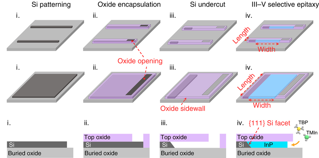
The Hong Kong researchers’ process for creating InP/SOI monolithic platform, including bars (top) and membranes (middle), for growing III–V photodetectors (and other devices) on silicon. (i) Patterning of silicon layer on silicon-on-insulator (SOI) wafer. (ii) Patterned bars or membranes are encapsulated by a top-oxide layer. (iii) The top-oxide layer is undercut using a wet-etching method, leaving a gap between the top oxide and the buried insulating oxide layer of the SOI wafer. (iv) InP is grown by lateral epitaxy, in-plane with the silicon device layer. [Image: Z. Yan et al., Light Sci. Appl. 10, 200 (2021), CC-BY 4.0] [Enlarge image]
An “ideal platform” for photonics?
To get around these quandaries, the research team, led by Keu May Lau of the Hong Kong University of Science and Technology, devised a new method to selectively grow the III–V material InP in parallel with the silicon device layer on an SOI wafer. The result, the researchers maintain, is “an ideal InP/SOI platform for implementing photonic functionalities.”
In the team’s approach (laid out in detail in a separate study), the 480-nm-thick silicon layer on the SOI wafer is first patterned into segments, and then encapsulated with a thin layer of oxide. Next, a wet-etching process undercuts the top oxide layer to create trenches beneath it, removing the silicon in selected areas and leaving a gap between the overlying encapsulating oxide and the insulating oxide layer beneath the silicon.
InP is then epitaxially grown, in a lateral direction, to fill the gap—creating an “InP-on-insulator” structure directly adjacent to the SOI one. The result, the researchers suggest, is a monolithic platform where InP bars and membranes of various lengths can sit in-plane with the silicon device layer, allowing for smooth light coupling with silicon waveguides while still taking advantage of the superior properties of InP (and other III–V materials) for high-speed photodetection.
Prototype devices
To test out its deposition scheme, the team fashioned photodetectors of a variety of detectors and configurations, using sequences of InP and InGaAs materials, on the monolithic InP/SOI base. The resulting devices, according to the researchers, put together all of the required criteria for high-performance photodetectors in data communications, with a 3-dB bandwidth beyond 40 GHz, high responsivity at telecom wavelengths, a broad operating-wavelength band and a low, 0.55-nA dark current.
The team also numerically simulated the photodetectors’ coupling efficiency with a butt-coupled silicon waveguide. It found that good light coupling between the III–V material and the silicon should be possible—something the researchers hope to demonstrate in future experiments.
The researchers conclude that the photodetectors that their new deposition process has enabled “are qualified candidates for future data communications in Si photonics.” And, they add, “the potential of achieving lasers on this platform further paves the way towards fully integrated Si photonics.”