
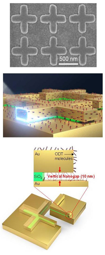
Researchers in Korea have devised a gold-and-dielectric metamaterial that can boost the efficiency of SEIRA, an infrared-spectroscopy method for detecting trace molecules. Top: Scanning electron microscopy (SEM) image of the metamaterial absorber top, showing cross-shaped antennas. Middle: Artist’s rendering of the microstructure of the metamaterial absorber. Bottom: Structure of the metamaterial absorber, including 10-nm vertical nanogaps and dielectric spacer material. [Image: Korea Institute of Machinery and Materials (KIMM)]
Researchers at two South Korean laboratories have devised a metamaterial-based absorber that can boost the molecule-detection efficiency of one type of infrared spectroscopy (Small Methods, doi: 10.1002/smtd.202100277).
The metamaterial absorber, which resembles a nanoscale wafer topped by equally thin Greek crosses, picked up a strong signal of a target molecule while performing surface-enhanced infrared absorption (SEIRA) spectroscopy, a technique for detecting trace molecules.
Spectroscopy for trace amounts
According to Jongwon Lee, associate professor of electrical engineering at Korea’s Ulsan National Institute of Science and Technology (UNIST) and one of the study’s lead authors, conventional methods such as Fourier-transform infrared (FTIR) spectroscopy cannot detect trace levels of analyte molecules. Because the molecules that have spectroscopic signatures in the mid-infrared region of the spectrum tend to have low absorption cross-sections, the FTIR technique requires a relatively large amount of material for a spectroscopic analysis.
SEIRA, a more recent method, works via the coupling between the high near-field enhancement induced in the engineered absorber structure and the vibrational mode of the target molecules, where the effective absorption cross-section is amplified, Lee says. Thus, only a tiny bit of the desired molecule needs to be present.
To make the SEIRA technique work properly, spectroscopists have studied absorbing structures with various types of nanometer-scale gaps to enhance the near field, but “but in most cases, the process cost is high and large area patterning and mass production are not possible,” Lee says.
The right pattern and thickness
Lee and his colleagues at both UNIST and the Korean Institute of Machinery and Materials (KIMM) designed a metamaterial absorber with a unit-cell structure consisting of a top cross-shaped gold nanoantenna, a gold backplane on the bottom, and a 10-nm-thick silicon dioxide spacing layer.
Although previous studies had indicated that the dielectric spacer had to be several tens or even hundreds of nanometers thick to optimize the SEIRA signal, Lee, Joo-Yun Jung of KIMM and their team found that the 10-nm gap was sufficient to realize high near-field intensities.
“In this configuration, the nanogap formed in the vertical direction can be easily controlled by adjusting the dielectric layer thickness, which is a great advantage over the recently developed SEIRA devices using high-cost processing such as e-beam lithography,” Lee says. “The proposed structure was processed using nanoimprint lithography, which enables a low-cost, large-area patterning, and the vertical nanogap was formed using isotropic dry etching, which indicates that the mass production of the proposed structure is possible.”
To further enhance the sensing efficiency of their SEIRA device, the researchers are studying new surface structures that are porous on the nanometer scale, with the ultimate goal of developing a sensitive and compact trace-material sensor.