
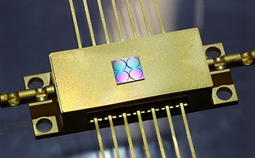
EPFL researchers have developed a CMOS-based fabrication process that yields very low-loss photonic microresonators and meter-long spiral waveguides. [Image: Jijun He and Junqiu Liu]
Scientists in Switzerland have demonstrated a new method for manufacturing photonic integrated circuits from very low-loss silicon nitride in high-yield wafers.
The researchers say the technology could allow frequency combs and other nonlinear devices to be mass-produced using conventional semiconductor fabrication techniques (Nat. Commun., doi: 10.1038/s41467-021-21973-z).
Microcombs and materials
Best known for underpinning modern electronics, straightforward silicon has also played a role in integrated photonics. It has been deployed widely, for example, in the form of data center interconnects.
But silicon has limitations when it comes to making nonlinear devices such as micro-scale frequency combs, or “microcombs.” These tiny ring-shaped resonators exploit the Kerr effect, a change in refractive index as light’s intensity varies. They convert a continuous-wave laser beam into a string of very short pulses whose frequency spectrum consists of a large number of very narrow and equally spaced lines.
Researchers have made microcombs from a range of materials, including lithium niobate, aluminum gallium arsenide, silicon carbide and diamond. But silicon nitride (Si3N4) appears particularly promising as it combines extremely low optical losses, strong Kerr non-linearity and is compact, among other things.
If silicon nitride waveguides are made very slender—with heights less than 100 nm—their losses can be as low as 0.3 dB/m. But this also limits their Kerr non-linearity. As such, most microcomb applications to date—including coherent communications, laser ranging, astronomical spectrometer calibration and optical clocks—have involved waveguides at least 700 nm thick.
Photonic Damascene process
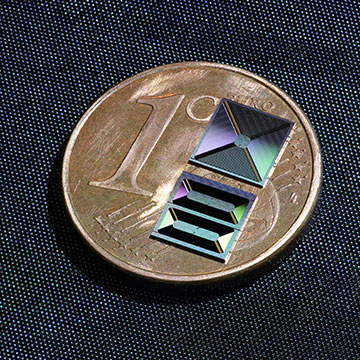
The integrated silicon nitride photonic chips are approximately 5×5 mm2. [Image: Jijun He and Junqiu Liu]
In the latest work, OSA Fellow Tobias Kippenberg, OSA student member Junqiu Liu and colleagues at the Swiss Federal Institute of Technology Lausanne (EPFL), show how 950-nm-thick microcombs with low loss can be made using standard CMOS fabrication techniques. Their “photonic Damascene process” relies on deep-ultraviolet lithography to boost throughput, stability and reproducibility compared with the electron-beam lithography widely used by other research groups. The process is so called as it resembles the way ornaments used to be made in Damascus, where metal was deposited in a mold and polished.
In this case, the material in question is silicon nitride rather than any metal. The researchers start by using the lithography, followed by dry etching and annealing, to precisely carve out waveguide channels in a silicon dioxide substrate. They then deposit a micrometer-thick film of silicon nitride and smooth out the top of it using what is known as etchback planarization, before carrying out further annealing and covering the circuit with silicon dioxide cladding.
Kippenberg and coworkers made dozens of 4-inch wafers, each comprising more than 200 5×5 mm2 chips that contain microresonators of varying size (resulting in microcombs with different line spacing). Using laser spectroscopy to measure the resonators’ linewidth, they found the devices had an average quality factor of around 30 million. They also measured the yield—the fraction of chips with a quality factor of at least 10 million—to be between 80% and 90%.
Toward even lower losses
To demonstrate that their process really is suited to high-yield, wafer-scale fabrication, the EPFL group also fabricated long spiral waveguides (such as those used to make delay lines). The team showed that it could fit a meter-long spiral into just a little over 6 mm2—an area some 300 times smaller than that needed for thin-core silicon nitride waveguides. The researchers note that the lowest loss they achieved—2.4 dB/m—was higher than that for the microresonators, which was around 1 dB/m, and attribute at least part of the difference to light-scattering defects caused by particles contaminating the wafer.
The researchers found that their waveguides’ inherent losses were dominated by Rayleigh scattering, and that losses could therefore be further reduced by optimizing the lithography and etching processes. Were they able to achieve ideal conditions and push those losses down to zero, such that the waveguides are limited only by absorption losses, they found that the quality factor in that case would be around 200 million—equivalent to just 0.15 dB/m.
Liu points out that fabricating fully-integrated microcombs will involve bringing together silicon nitride chips with others made from different materials—such as silicon and indium phosphide, to create a laser gain medium. He says that his group and another from the University of California Santa Barbara has in fact developed a CMOS-based technology to fabricate such integrated microcombs on a silicon substrate—yielding thousands of microcombs from a 4-inch wafer.