
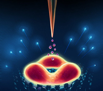
Researchers have developed a single-photon emitter that uses the fine tip of a scanning tunneling microscope (STM) to shoot electrons into precisely located atomic defect centers in a 2D material, stimulating the creation of individual photons. [Image: Ignacio Gaubert/LBL News Center]
Many technologies in the quantum-enabled future, such as quantum communications, rest on an elusive goal: finding materials that can pump out identical single photons with well-defined optical properties on demand—and that are capable of on-chip integration. A team of researchers from the United States, Germany and Spain has developed a system that it believes may offer an answer (Sci. Adv., doi: 10.1126/sciadv.abb5988).
The team’s approach uses defects in a 2D material, tungsten disulfide (WS2), as individual emission sources. The researchers have developed techniques to create such defects at precise locations, and to use the hyperfine gold tip of a scanning tunneling microscope (STM) to inject excitation electrons into these atom-scale centers. The same gold tip serves as a plasmonic antenna for shunting out the photons emitted as a result of the electron excitation.
The result is a sort of electrically triggered single-photon gun, which fires out individual, identical photons on demand, from a well-defined material defect that behaves much like a quantum dot. And the team says it can tune the properties of the emitted photon by adjusting the applied bias voltage.
Quantum emitter quest
The material used by the team, WS2, is one of a class of atomically thin, semiconducting 2D materials, called transition metal dichalcogenides (TMDs), with favorable optical properties (see “Optoelectronics in Flatland,” OPN, July/August 2015). Previous studies had suggested that these materials might indeed function as quantum emitters. In recent experiments, for example, quantum emission centers have been demonstrated in TMDs such as tungsten diselenide (WSe2) and molybdenum diselenide (MoSe2).
In those cases, the photons emitted from the material apparently arose from local confinements of energy at residual strain centers, randomly distributed in the material. The problem for quantum technology has been in nailing down the position of those emitters—and in ensuring that the photons generated from them had identical optical properties, a key requirement for single-photon sources in quantum technology.
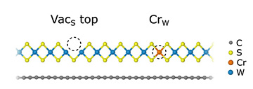
The team used precisely located defects—including the substitution of chromium for tungsten atoms, and the creation of sulfur vacancies—in a layer of tungsten disulfide atop an atomically thin layer of graphene (gray chain in diagram). [Image: B. Schuler et al., Sci. Adv., doi: doi: 10.1126/sciadv.abb5988 (2020); CC-BY-NC 4.0]
To get past those problems, the researchers behind the recently reported work looked at a different approach. Specifically, they decided to create individual quantum emitters at well-defined points in the material, through the judicious substitution of chromium for tungsten at some locations and through the removal of individual sulfur atoms at other places, to create a “sulfur vacancy” in the crystal lattice.
Such a system, the team reasoned, would allow precise location of the single-photon emitters in the WS2 sheet. And, because they arose from identical crystal defects, the emitted photons would all share the same optical properties, making them effectively identical with one another.
Foundry work
The researchers created the photon-emitting material by using chemical vapor deposition to lay down a single layer of WS2 islands on a layer of epitaxially grown graphene—another 2D material—which in turn sat on a silicon carbide substrate. As grown, the material included a number of intentional defects, including the substitution of chromium for tungsten in some sites. Then, the team employed a high-temperature annealing technique to create regularly spaced sulfur vacancies in the lattice as well.
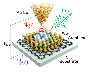
In the team’s concept, an STM tip pumps electrons into an individual defect centers to excite a transition there, and then acts as a plasmonic antenna to channel out individual photons from the excited state. [Image: B. Schuler et al., Sci. Adv., doi: doi: 10.1126/sciadv.abb5988 (2020); CC-BY-NC 4.0]
Next, the researchers used a gold-coated STM tip to electrically stimulate the defect centers they had created. Under the scheme, electrons are pumped from the tip into precisely located, single defect centers, where the relaxation of the excited defect results in the emission of a single photon. The tip then acts as a plasmonic antenna, guiding the emitted photon to an optical detector, where its wavelength and position are recorded.
The bias voltage between the tip and the sample determines the electron injection energy. Thus, the voltage can be used as a control knob for switching between different transition states in the defect center, and thereby tweaking the optical properties of the emitted photon.
One defect, one electron, one photon
The team was able to use this system to map photon emissions in the thin material at resolutions of less than an angstrom (0.1 nm). That effectively means atomic resolution, and is, according to the research team, the highest spatial resolution thus far reported in this sort of work.
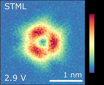
The team was able to map the intensity and location of photons emitted from the thin-film material while a voltage was applied. Color key shows photon counts per second, ranging from zero (blue) to 1,500 (red). [Image: Berkeley Lab]
Of particular interest, the researchers also observe that their approach—which uses single electrons to coax single photons out of single defect centers—allows them “to avoid averaging and environmental decoherence effects.” This, they believe, opens up the prospect of highly refined control of quantum properties through control of the electron injection, eventually enabling “on demand spin-polarized single-photon emission in a solid-state tunneling device.”
In a press release accompanying the work, the team lead, Alexander Weber-Bargioni of the Molecular Foundry at the Lawrence Berkeley Lab (LBL), USA, held that the group’s demonstration marks “a big step in the quest for integrable quantum technologies.” The team believes that its techniques offer a scalable strategy for creating single-photon emitters for quantum networks and quantum simulations, and is working on ways to put the approach into use in these areas.
In addition to scientists at LBL, the work also included contributors from the Technical University of Munich, Germany, and ICFO–Institut de Ciències Fotòniques, Spain.