
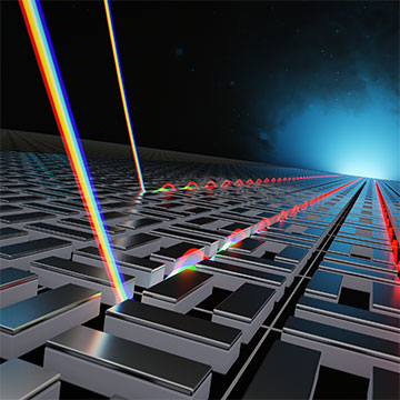
Simple grating lines arranged in a checkerboard pattern could enhance the performance of thin-film solar cells. [Credit: David Zecca, davidezecca.artstation.com]
One strategy to reduce the cost of solar cell production is minimizing the amount of active material in the device. Thin-film solar cells do just that, but they suffer from low light absorption, which limits their performance.
Light-trapping techniques such as incorporating photonic and plasmonic nanostructures into the various surfaces of thin-film solar cells aim to offset this disadvantage. In a new study, a team of researchers from the United Kingdom, Portugal and Brazil has demonstrated that arranging simple grating lines can yield the same high performance as more sophisticated designs (Optica, doi: 10.1364/OPTICA.394885).
Nanostructures for better absorption
To meet the requirements of global energy demand, photovoltaics must deliver a high power conversion efficiency coupled with low production costs. Thin-film solar cells could feasibly reduce the price of module production, and solar power in general, since they only require a micron-thick layer of active material. However, such a slim layer means low-energy photons are less likely to be absorbed.
“As a thinner layer absorbs less light, optical concepts [such as nanostructures] must counter this loss,” said Christian Schuster, senior author and researcher at the University of York, U.K. “Photonic solutions here offer the possibility of efficiency enhancements at lower costs, enabling optically thicker yet physically thinner solar cells.”
Nanostructures incorporated into a thin-film solar cell surface can achieve the goals of light trapping to enhance its overall efficiency. For instance, they may channel light toward the photovoltaic material and prevent it from escaping outwards, or reduce optical losses by acting as an antireflection coating.
The checkerboard solution
After running a number of computational simulations, Schuster and his colleagues noticed that the arrangement of grating lines could outperform more complicated nanostructured arrays of 3D shapes. Their simulation contained a test solar-cell structure composed of a micron-thick crystalline silicon absorber material with an ideal back reflector.
They focused on different forms of a checkerboard pattern resulting from the displacement and 90-degree rotation of periodic grating lines. All grating lines were etched on the front surface of the cell. Impressively, this quasi-random structure was able to enhance the bulk current of the solar cell by 125%.
The simplicity of their design has practical advantages for industrial mass production, and its reduced surface area compared with other nanostructured arrays will lead to reduced surface-recombination effects. Its large rectangular features also contribute to a high robustness to fabrication imperfections.
“We strongly believe the photonic nature of our design principle along with its simplicity can greatly appeal to industry but also inspire revived initiatives to explore light-management approaches from a new perspective,” said Schuster.