
Researchers have developed a precision spray-coating method that produces multilayer perovskite absorber for advanced solar cell designs and could be scaled up. [Image: Pongsakorn Kanjanaboos, Mahidol University]
The crystalline semiconductors known as perovskites have generated great interest as potential building materials for solar cells, but to make them practical for widespread use, researchers must develop efficient manufacturing processes to handle them. Scientists in Thailand have devised a spray-on method of applying precise layers of perovskites to substrates to make stable, high-performance photovoltaic structures (Opt. Mater. Express, doi: 10.1364/OME.391546).
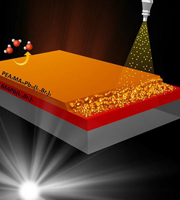
Perovskites come in numerous chemical formulas, usually with two different cations and three anions. The team at Mahidol University’s School of Materials Science and Innovation focused on mixed halide perovskites, which include some combination of bromine or iodine atoms as the anions. This type of semiconductor compound has a color ranging from brown to orange and is somewhat transparent to light—useful if someone wanted to design decorative windows that also generate electricity.
Issues with past efforts
At the scales of a few hundred nanometers, semiconductor shapes and layers determine the function of a device. Creating light absorbers with different types of perovskites in three or more layers would allow many complex designs that have not been possible previously, says Pongsakorn Kanjanaboos, the Mahidol team leader.
Since perovskites can be made into a liquid solution for processing, spray deposition seems like an obvious manufacturing method, but the technique was difficult to predict and control. Previously, Kanjanaboos’ group and other scientists could coat a second layer of perovskite on top of a base layer only by quickly exposing the lower layer to some chemicals. These processes led to surface passivation—the droplets of the upper layer would partially re-dissolve the previously dried lower layer, according to Kanjanaboos. Scientists lacked precise control of the capping layer’s thickness and its effect on the lower layer.
Sequential spraying for the win
The Mahidol researchers dubbed their technique “sequential spray deposition,” or SSD. Kanjanaboos and his colleagues used two air jets at 45-degree angles to a substrate heated to 100 ºC to spray fine droplets of perovskite solution onto the substrate. The team kept the air in the experiment space humid—45% to 50% relative humidity—to keep the layers more stable.
Some halide perovskites—with three iodine atoms per molecule—have better electrical properties but less stability with respect to environmental conditions. Kanjanaboos and his team laid down that type first, then spray-deposited a 90-nm-thick capping layer as soon as the 400-nm-thick lower layer was dried. The group made only two layers, but they say that many more layers could be stacked with precise control of thicknesses and rates of deposition for each layer.
Kanjanaboos says the new technique opens new paths for not just perovskite solar cells, but also the whole spectrum of perovskite electronics like perovskite LEDs, photodetectors, lasers and so on. “We have very interesting device structures in mind,” he adds. “SSD allows us to fabricate them for the first time.”