
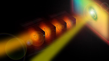
Artist’s rendering of a mid-infrared probe beam (orange) and a near infrared pump beam (yellow) striking a CCD sensor. The energies of photons in the pump and probe beam combine to create a photocurrent in the sensor, allowing the MIR signal to be imaged using an ordinary silicon-based camera. [Image: D. Knez et al.]
While light sources for mid-infrared (MIR) sensing have come a long way in recent years, cameras for MIR imaging—to create, for example, detailed chemical maps of a sample—remain costly and imperfect. As an alternative, some researchers have played with various approaches to upconverting the MIR signal to visible wavelengths, so that it can be detected by an ordinary silicon-based CMOS or CCD camera. These schemes, however, can be fussy, requiring multiple realignments of nonlinear crystals in a single experiment to get a good MIR-derived image.
A team of scientists at the University of California, Irvine, USA, has now gotten around those problems through a technique that uses the CCD chip itself as the nonlinear element, dramatically simplifying the process of imaging MIR data via a conventional silicon-based camera (Light Sci. Appl., doi: 10.1038/s41377-020-00369-6). The researchers believe that the approach—fast enough to capture MIR videos of moving objects—could offer a route to practical and compact, room-temperature MIR imaging for biomedicine, industrial testing, environmental monitoring and other applications.
Molecular fingerprints
The MIR wavelength band, commonly defined as the range between 2 and 20 µm, is of particular interest because it includes the so-called molecular-fingerprint region, where many important molecules sport strong fundamental vibrations. That makes the MIR band a sweet spot for spectroscopic chemical imaging and mapping.
MIR sensing has surged forward in recent years in part due to advances in MIR light sources (particularly quantum cascade lasers) used to excite these molecular vibrations. MIR cameras for imaging haven’t progressed as fast, however. Common cameras that operate natively in the MIR, while they can be exquisitely sensitive, are costly, somewhat temperamental beasts prone to thermal noise, and need to be cooled to frigid, cryogenic temperatures to overcome that problem. That doesn’t make for the most convenient field setup.
Upconverting to the visible
To get to something a bit more practical—and less expensive—research groups in the past decade have looked at an alternative to native MIR imaging: converting the MIR light to visible colors that can be detected at room temperature using a conventional silicon-based camera. One common approach has relied on sum-frequency generation (SFG), in which photons from the MIR radiation interact with photons from a strong near-infrared (NIR) pump beam in a nonlinear crystal, to create new photons at the frequency sum of the two input beams.
In this way, SFG can convert the MIR signal to visible wavelengths that can be sensed and analyzed using an ordinary CCD camera. The process works—but there’s a hitch. The SFG process by nature requires careful phase-matching of the MIR input and NIR pump beams. That means that a single MIR imaging experiment can require multiple reorientations and realignments of the nonlinear crystal, as well as postprocessing of each measurement to build up the final image.
A simpler setup?
The Irvine team, led by Dmitry Fishman and OSA Fellow Eric Potma, looked at a potentially simpler alternative—using the CCD camera chip itself as the nonlinear element. The specific nonlinear process the researchers explored is nondegenerate two-photon absorption (NTA). In this process, photons from an MIR probe beam and an NIR pump beam are absorbed by a wide-band-gap semiconductor to push electrons into the conduction band, thereby directly creating charge carriers in the semiconductor.
The scheme, if it could be made to work in silicon, would eliminate the need for phase-matching of the pump and probe beams. Indeed, it would do away with the need to have a separate nonlinear crystal at all, simplifying the setup.
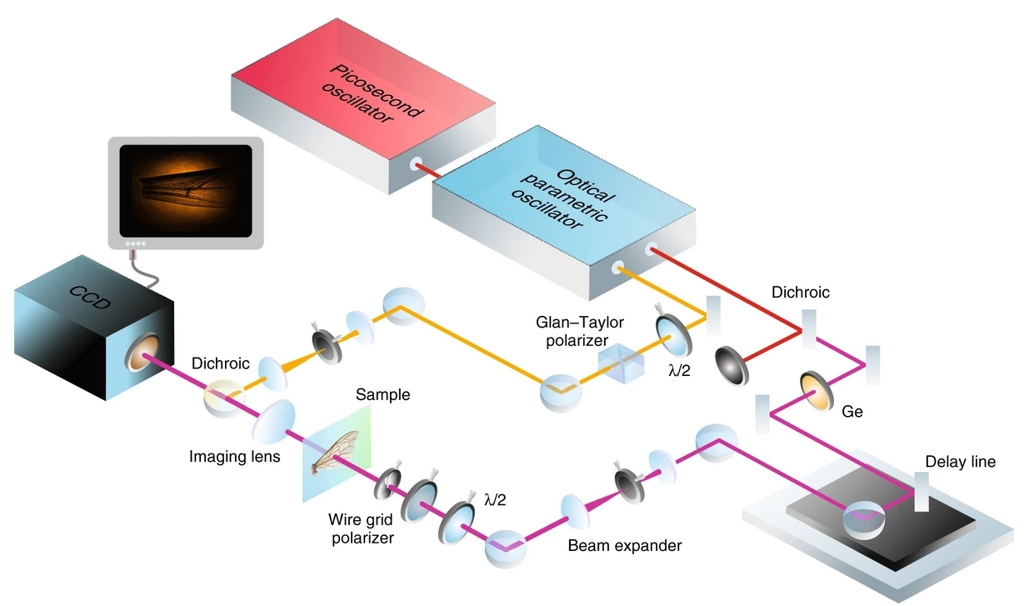
Schematic of the Irvine team’s wide-field MIR imaging system, based on non-degenerate two-photon absorption in a silicon-based CCD camera. [Image: D. Knez et al., Light Sci. Appl., doi: 10.1038/s41377-020-00369-6 (2020); CC BY 4.0] [Enlarge image]
To establish that NTA would work for MIR sensing in silicon, the team first tested the system out with a simple, single-pixel silicon photodiode, successfully carrying out simple MIR spectroscopy on a known sample. Then, for a more realistic test, they replaced the photodiode with a CCD camera. In the setup, an optical parametric oscillator (OPO) is used to create both the MIR probe beam and the NIR pump beam. The MIR beam is passed through the sample, while the NIR pump is directed, via a dichroic mirror, to overlap with the MIR beam immediately before both find their way into a 1392×1040 CCD sensor—where photons from the two beams give rise to the photocurrent used to create the image.
Toward real-time, MIR-derived videos
Using the setup, the team was able to capture MIR-derived images at exposure times of around 100 ms, of samples including polymers and biological materials such as a bee’s wing. The exposure time was fast enough to enable videos of moving targets such as live nematode worms. And the system required no crystal alignment or postprocessing of images, setting up the possibility of its use in real-time MIR imaging.
The system still is in need of some refinement. One obvious wrinkle is the need for synchronized pump and probe pulses; the team used an OPO in its proof-of-concept experiments, but that solution may not be ideal for a compact, cheap system. The researchers believe, however, that “recent developments in MIR light source technology” could offer alternatives to OPOs that could enable a somewhat more compact, less costly setup.
Meanwhile, the team stresses that the system uses direct MIR light, rather than light upconverted via a separate nonlinear crystal, as its input—a gain in simplicity—and takes advantage of the high pixel densities, large imaging areas and mature ecosystem of silicon CCD sensors and CMOS cameras. These advantages, the team concludes, could make the system a nice fit for fast MIR imaging in a range of contexts, including environmental sensing, bioimaging and industrial testing.