
![]()
Far field pattern of the Japan team’s UV-C laser diode, projected onto a fluorescent screen. [Image: © 2019, Asahi Kasei Corp. and Nagoya University]
Researchers in Japan have developed a semiconductor laser diode that operates in the deep ultraviolet, at a wavelength of 271.8 nm—the shortest wavelength, according to the authors, of any current-injected laser diode yet reported (Appl. Phys. Express, doi: 10.7567/1882-0786/ab50e0). The team believes that such deep-UV diode lasers constitute “potential enabling devices” for a variety of applications in sensing, disinfection and biomedicine.
Tough threshold to cross
The past decade has seen huge advances in light-emitting diodes (LEDs) for the deep UV, with devices pushing down into emission wavelengths as low as 210 nm. Those developments have rested largely on the advantages of so-called group III nitride materials—particularly AlGaN, emissions from which can be tuned to create LEDs covering virtually the entire UV spectral range.
But extending that progress in LEDs to push semiconductors lasers into the deep UV has proved a tougher proposition. Demonstrated UV laser diodes thus far have not gotten to wavelengths shorter than 336 nm, according to Chiaki Sasaoka of Nagoya University, one of the new study’s senior authors. One reason is that, when an active layer of AlGaN crystals are grown on conventional substrates such as SiC or sapphire, it can lead to the formation of internal dislocations and cracks, degrading the quantum efficiency of the active layer.
An even more fundamental hurdle lies in the diode architecture itself. A laser diode includes a quantum well at the center, where the laser light is created by the radiative combination of negatively charged electrons from the diode’s so-called n layer with positively charged electron vacancies or “holes” from its p layer. Creating a deep-UV laser diode requires that the central quantum well be surrounded by thick cladding layers that both can confine light in the quantum well, and are electrically highly conductive to facilitate the current-driven migration of electrons and holes.
That combination, it turns out, has been difficult to achieve in AlGaN alloys—particularly in the p or hole-transport layer of the stacked diode structure. That’s because the conductivity of positively charged holes tends to go down as the percentage of aluminum in the mix goes up.
Improved substrate and doping
The researchers behind the new work—led by Sasaoka and 2014 Nobel Physics laureate Hiroshi Amano of Nagoya University, working with others at Nagoya and at the Asahi Kasei Corporation, Japan—drew on several techniques to get around these limitations.
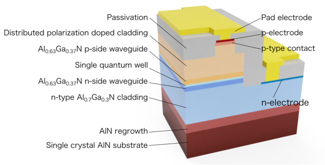
Cross-sectional structure of the UV-C semiconductor laser diode. [Image: © 2019, Asahi Kasei Corp. and Nagoya University] [Enlarge image]
One started at the substrate, for which the team used an extremely high quality, 2-inch single crystal of aluminum nitride (AlN), obtained from the U.S. firm Crystal IS. The high-quality AlN substrate, with a very low internal dislocation density, avoided the material problems that tend to sap the quantum efficiency of deep-UV lasers built on other substrates.
On top of that AlN substrate, the team epitaxially grew a stack of materials to create the laser diode architecture. At the center of the stack is a thin, 9-nm single quantum well tuned to emit at 270 nm, sandwiched between 50-nm-thick p- and n-side AlGaN layers acting as waveguides. On the n (electron-mobile) side, a 350-nm-thick AlGaN layer, conventionally doped with silicon impurities, acted as the lower cladding layer to hem light into the waveguide.
For the cladding on the upper, p (hole-mobile) side, the team used a very different approach for the semiconductor doping—so-called distributed polarization doping (DPD). In this approach, rather than being doped with impurities, the material’s percentage of aluminum is varied layer by layer as the cladding is deposited. The result is a 320-nm-thick n-side AlxGa1-xN cladding layer that’s graded compositionally from pure AlN at the bottom to Al0.7Ga0.3N at the top.
The compositional grading, it turns out, gives rise to internal polarization fields in the cladding layer that boost the conductivity for positively charged holes in the layer. That permits the high current densities needed for electrically pumped laser operation—while still allowing a sufficiently thick, Al-rich cladding layer for good light confinement in the central quantum well, where the electrons and holes combine radiatively to create the laser light.
Moving toward real-world applications
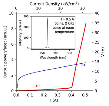
Current–voltage (I–V, blue) and the emission power (red) characteristics of the team’s deep-UV laser, under pulsed-current operation. The inset shows the sharp emission at 271.8 nm. [Image: © 2019, Asahi Kasei Corp. and Nagoya University]
The team found that the structure lased at 271.8 nm—“the shortest wavelength reported so far” for a current-injection laser diode, according to the authors—at room temperature, and at a pulsed threshold current of 0.4 A. The authors also point out that the graded valence-band profile enabled by DPD led to a “remarkably low operating voltage” of 13.8 V for the diode at that current.
The lasing wavelength puts the new diode squarely in the so-called UV-C band (200–280 nm), which has piqued interest for applications such as disinfection in healthcare settings, treating of certain skin conditions (such as psoriasis), and environmental sensing. The researchers are now working with Asahi Kasei Corporation to get to continuous deep-UV emission from the device at room temperature, to set the diode up for real-world applications.