
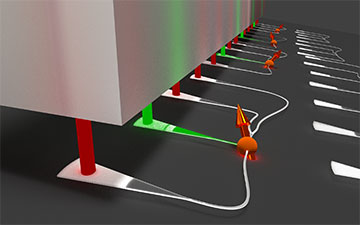
Researchers have shown how to simultaneously operate multiple sources of single photons in the form of nitrogen–vacancy centers within nanodiamonds integrated into a nanophotonic network. [Image: P. Schrinner/AG Schuck]
The quantum technology of tomorrow will likely require large numbers of individually accessible components to be integrated onto monolithic photonic chips. Scientists have made significant progress in joining up single-photon detectors and other components, but adding sources of single photons has proved a bigger challenge.
Now, researchers in Germany have integrated several nanometer-sized pieces of diamond into a nanophotonic network and shown how each can be made to emit single photons independently of the others. They say that in the near-term their technology should be well-suited to producing sensitive quantum-based magnetometers (Nano Lett., doi: 10.1021/acs.nanolett.0c03262).
Diamonds and quantum technology
Diamond can be turned into a single-photon source by creating what are known as nitrogen–vacancy centers. These involve the replacement of two carbon atoms in the diamond lattice by a nitrogen atom and a gap. The gap contains an unpaired electron that can bind to an external electron to form a quantum-mechanical spin system that can be made to fluoresce—emitting a stream of single photons at red wavelengths when probed by green light.
These vacancy centers are being investigated by scientists around the world for use in a range of quantum technologies, including computation, communication and sensing. However, like other sources of single photons, it has so far not been possible to operate large numbers of these crystal defects in parallel and independently of one another.
An integrated nanophotonic network
To show how this could be done in principle, Carsten Schuck and colleagues at the University of Münster have etched photonic circuits from thin films of tantalum pentoxide-on-insulator laid on top of a silicon substrate. Each nanophotonic device consists of several waveguides connected to optical fibers at one end and a photonic crystal cavity—containing the vacancy center—at the other.
To create the cavity, the researchers coated the chip with a polymer resist and then used electron beam lithography to cut a series of 240-nm-wide holes at regular intervals along a tapered section of the tantalum pentoxide. They then filled the center holes with 35-nm-diameter pieces of artificial diamond by placing these “nanodiamonds” in a deionized water solution, dropping the solution into the holes, waiting for the water to evaporate and then using acetone to remove excess nanodiamonds as well as any remaining resist.
To put their technology to the test, Schuck and co-workers exposed a nanodiamond-containing cavity to 532-nm laser light either incident from a macroscopic lens or delivered via a dedicated waveguide oriented at right angles to the cavity. In both cases they observed a sharp peak in the cavity's emission at around 705 nm and also confirmed that the emitted photons had undergone antibunching—a nearly uniform delay between one photon and the next that is characteristic of a single quantum emitter.
Toward measuring magnetic fields
The researchers then demonstrated how their devices could, in principle, be used as sensitive detectors of magnetic fields. When exposed to microwaves of a certain frequency, the electron pair in a nitrogen–vacancy center enters a pair of degenerate states that diminishes its fluorescence in the presence of green laser light. But if the device is then immersed in a magnetic field, the degenerate states split and the microwave resonance frequency changes—allowing magnetic field strengths to be measured.
Although Schuck and colleagues didn’t expose their devices to magnetic fields, they did reveal the characteristic microwave-induced drop in output. They first tested a single vacancy center by positioning a copper wire attached to a microwave generator close by and then sweeping the microwave frequency while keeping a continuous-wave green laser switched on. They then repeated the exercise with two devices stimulated simultaneously—one of which contained multiple vacancy centers.
While the researchers saw the fluorescence intensity dip at the expected 2.88 GHz when using a single device, they observed slight shifts of the microwave resonance in the second test. They say that in the case of the single vacancy center that was probably due to greater internal pressure—another parameter that can potentially be measured with such systems—while they reckon that in the other case the various nanodiamonds contributing to the signal were likely oriented in different directions.
For this technology to be deployed in real magnetometers, they say that further work will be needed to characterize and calibrate the nanodiamond devices. They add that any applications will benefit from more vacancy centers per device as well as pulsed lasers to both excite the electronic system and record its emissions. Nevertheless, they argue that their results “show on a qualitative level that far-separated independent devices can be operated simultaneously.”