
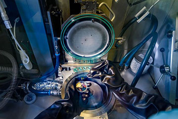
Researchers used this metal organic vapor phase epitaxy (MOVPE) to grow hexagonal silicon-germanium crystals that can emit light across a range of wavelengths. [Image:Nando Harmsen, TU/e]
For about 50 years, scientists have dreamed of making a silicon laser, a device that would emit light cheaply and efficiently using the material ubiquitous in modern electronics. Built directly into integrated circuits, such a laser could allow photons to replace electrons for much on-chip communication—potentially allowing faster, cooler processing in data centers and beyond.
Now, researchers in Europe have shown how a silicon laser might be built by fabricating a direct-band-gap semiconductor from nanowires of silicon-germanium alloys with a hexagonal crystal structure (Nature, doi: 10.1038/s41586-020-2150-y).
Issues with silicon
Direct-band-gap materials such as gallium arsenide and other compound semiconductors have excellent optoelectronic properties. Incoming photons can generate currents by boosting electrons from the valence band to the conduction band, while excited electrons can drop back down to the valence band and emit light. However, these materials are quite expensive and they must somehow be connected to the silicon—usually via bonding or off-chip wiring.
Silicon itself is very cheap, plentiful and amenable to mass production, but its crystal structure is such that valence and conduction bands do not line up with one another. Because electronic transitions generate vibrations in the crystal lattice, electrons that shed energy generally don’t yield photons, making silicon a very inefficient light emitter. (Likewise, absorbed photons usually don’t excite electrons, meaning that silicon solar cells have to be far thicker than devices made from compound semiconductors.)
In the 1970s, it was proposed that the band gap in silicon and silicon alloys could be made direct by exposing the materials to a periodic electric potential. That idea was put into practice two decades later by researchers at Daimler-Benz in Germany, who built up crystals from alternating layers of different atoms. However, the resulting material was still too inefficient an emitter or absorber to be useful.
A hexagonal solution
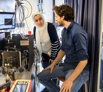
First authors Elham Fadaly (left) and Alain Dijkstra (right), in the optical lab where the SiGe alloy’s emission properties were tested. [Image: Sicco van Grieken, SURF]
In the latest work, Erik Bakkers and colleagues at the Eindhoven University of Technology, Netherlands, instead keep the atomic composition constant but alternate the way that those atoms are stacked. They do so by replacing silicon’s usual cubic lattice structure with a hexagonal one. This doubles the number of atoms in the crystal’s unit cell, which halves the size of the corresponding momentum unit cell and, in germanium or a silicon–germanium alloy, alters the material’s conduction band such that it yields a direct band gap.
Bakkers and his co-workers had, in fact, already attempted this in 2015. They used a gallium phosphide nanowire as a template around which they grew hexagonal crystal shells of silicon–germanium alloys. However, defects in those crystals, caused by strain in the lattice, prevented light emission. Having since gotten together with other researchers in Germany and Austria, they have altered the design process so that they instead craft their silicon–germanium crystals using a 35-nm-diameter nanowire of gallium arsenide.
The researchers carried out experiments involving alloys with a range of compositions—the silicon content varying from 0% to 35%. They say that structural microscopy and luminescence data showed that these hexagonal crystals do indeed exhibit a direct band gap. In fact, by exposing the nanowires to laser light, they found that the crystals can emit almost as efficiently as gallium arsenide and indium phosphide—with the wavelength of the emitted light depending on the amount of silicon in the alloy.
Future applications
In a commentary accompanying the research, Anna Fontcuberta i Morral, EPFL, Switzerland, says that the range of photon energies emitted—0.3 to 0.67 electronvolts—would make the technology well suited to chemical sensing and optical communications. She reckons it might also be used to make light detectors operating at mid-infrared wavelengths, perhaps leading to high-powered lidar systems for self-driving vehicles—which would, she points out, allow those vehicles to detect objects a long way off and therefore travel at speed.
As for creating a laser from the silicon-alloy nanowires, Bakkers believes that “if things run smoothly” he and his colleagues might achieve that by the end of the year. But he acknowledges that they must still find a way of integrating their hexagonal silicon into the cubic crystals used in microelectronics. They are also designing the laser cavity, he adds.