
Jelena Vuckovic at FiO+LS 2019. [Image: Alessia Kirkland]
Integrated nanophotonics promises a generation of spiffy, miniaturized optical components that could drive new capabilities, in applications from communications to lidar to quantum technology. But getting there requires packing huge optical functionality into a very small footprint—and that’s been a formidable challenge in design, fabrication and just plain time.
In a “Visionary Speakers” talk at Frontiers in Optics+Laser Science 2019, Jelena Vuckovic of Stanford University, USA, showed how her research group and others are attacking the problem with techniques that can slash the design time of creating fab-ready nanophotonic components. The secret: Put some clever computer optimization, blazing-fast custom-written software, and machine learning on the case.
The quest to beat electronics
The fundamental question, as Vuckovic put it, is “really whether photonics can go through same revolution that electronics went through in the 20th century”—when Moore’s law, fabrication advances and the maturing of the semiconductor industry shrank computers from room-size to pocket-size. Thus far, however, photonics has not been especially cooperative. Devices, Vuckovic noted, tend to be large—“tens of microns per component”; they’re also sensitive to the vagaries of fabrication defects and temperature swings, and even the best generally require manual tuning of a few design parameters.
As a result, according to Vuckovic, even when engineers manage to shrink photonic components down to the length scale of electronics, the photonic devices frequently don’t outperform their electronic counterparts. Some key elements, such as couplers, can have efficiencies of 50% or lower.
From a lifetime to an hour
Vuckovic thinks we can do a lot better. And the key, she said, it to look at the design of photonic components in a fundamentally different way—as an inverse problem subject to computer optimization.
To illustrate the approach, she diagrammed a simple targeted optical-component—a 2-D mode converter, with a 2.5×1.5-micron footprint, that can change an input waveform in first-order mode to an output second-order-mode waveform with greater than 90% efficiency. In her diagram, the “guts” of the device, where the mode conversion actually takes place, is the proverbial black box. Indeed, she said, every photonics design problem boils down to “finding the black box that will do a particular transformation.”
One approach to solving for the black box, Vuckovic explained, would be breaking the region into a 2-D array of 100-nm pixels, and then applying brute force, computing all possible combinations until one that works emerges. “In principle, if you’re lucky you’ll solve the problem that way,” she said. But in practice, the parameter space is so large that “you’ll not be able to solve the problem in your lifetime.”
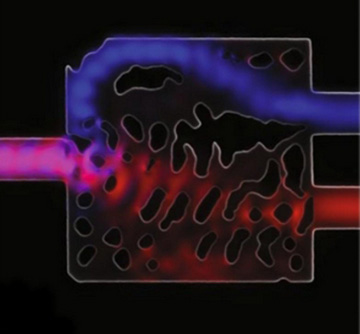
[Image: Stanford Nanoscale and Quantum Photonics Lab]
Instead, Vuckovic’s team has developed methods and computer codes that replace this “blind search” with what she calls a “physics-guided search,” in which high-speed electromagnetic-equation solvers iteratively calculate the optical behavior in the box and, guided by machine-learning techniques, converge on an answer. Using that approach, Vuckovic said, “the design of a physical device of this type”—that is, the simple mode splitter—takes not a lifetime, but “about an hour.”
Counterintuitive solutions
One key to this speed is the work Vuckovic’s team has done on optimizing the electromagnetic solvers—work that has resulted in a software package that runs much faster than commercial equivalents. And she believes a tenfold additional speedup might be possible; that would cut the a design/optimization time for the hypothetical sample component from an hour to only six minutes.
Interestingly, said Vuckovic, using this approach “you end up with structures that aren’t intuitive at all … but that outperform other devices on many figures of merit.” And the devices are computer-optimized to be robust against errors and temperature changes. Vuckovic noted that the team’s software suite—Stanford Photonics Inverse design Software (SPINS)—has been licensed to several major companies, with a separate suite (SPINS-B) released as open-source software for the research community.
Fab ready
Vuckovic and her team have spent much of the past several years working to establish that these unconventional design techniques are compatible with high-throughput fabrication and industry semiconductor foundries. For that task, her lab has worked with commercial and nonprofit foundries including Imec, Global Foundries and AIM Photonics. And the results, she said, have been good.
She showed data for a number of classical photonics devices, including a spatial mode splitter/converter, a three-channel wavelength demultiplexer, and a 50-50 beam splitter, for which the lab used its inverse method on the design, and then sent the designs without further modification to a conventional silicon foundry. In all cases, the foundry returned devices with performance metrics that—without any post-tuning—agreed quite well with both numerical models and the lab’s own custom-fabricated devices. “We’re convinced this is fully compatible with foundry fabrication,” even of larger cirucits, Vuckovic maintained.
New horizons: Classical …
![]()
Jelena Vuckovic at FiO+LS 2019. [Image: Alessia Kirkland]
According to Vuckovic, the inverse-design techniques that her team has honed an also be turned to create new functionalities—to “build systems that you couldn’t otherwise build.”
The group has put that idea to work in building an on-chip isolator (a notoriously difficult problem in integrated nanophotonics), in a collaboration with Andrea Alù of City College of New York, USA. Such a device, she suggested, has the potential to replace chains of gated switches and oscillators in lidar systems with a much simple setup consisting of two micro racetrack resonators. And the team has put the inverse approach to work in problems such as creating on-chip particle accelerators, and in dispersion engineering, an essential task for designing nonlinear elements and new kinds of hyper-miniaturized components such as on-chip frequency combs.
“Even the best dispersion designer can only go so far using manual dispersion tuning,” Vuckovic said. “If you use optimization, you can go beyond your intuition, and let the computer design the system that will work for you.”
… and quantum
Vuckovic closed her talk with a look at some of her team’s activities in applying inverse-design techniques to problems in quantum optics. Here, she noted, the constraints are even tighter—a tiny number of photons, very low powers, and the need to keep losses ultra-low to avoid destroying delicate quantum signals.
All of these quantum systems are based on the same elements – homogeneous qubits with optoelectronic interfaces, and optial interconnects that are efficient (for entanglement without loss). The team has been exploring these problems, particularly in diamond color-center systems and in the emerging material of silicon carbide (SiC). Vuckovic called SiC “the ideal photonics material,” sporting good optical, quantum and fabrication properties. And her team is working hard to realize that promise, by solving problems such as how to make thin films out of SiC—a hurdle the team cleared only recently.
“It’s all quite exciting,” said Vuckovic. “I think we can build quantum simulators and networks using this platform.”