
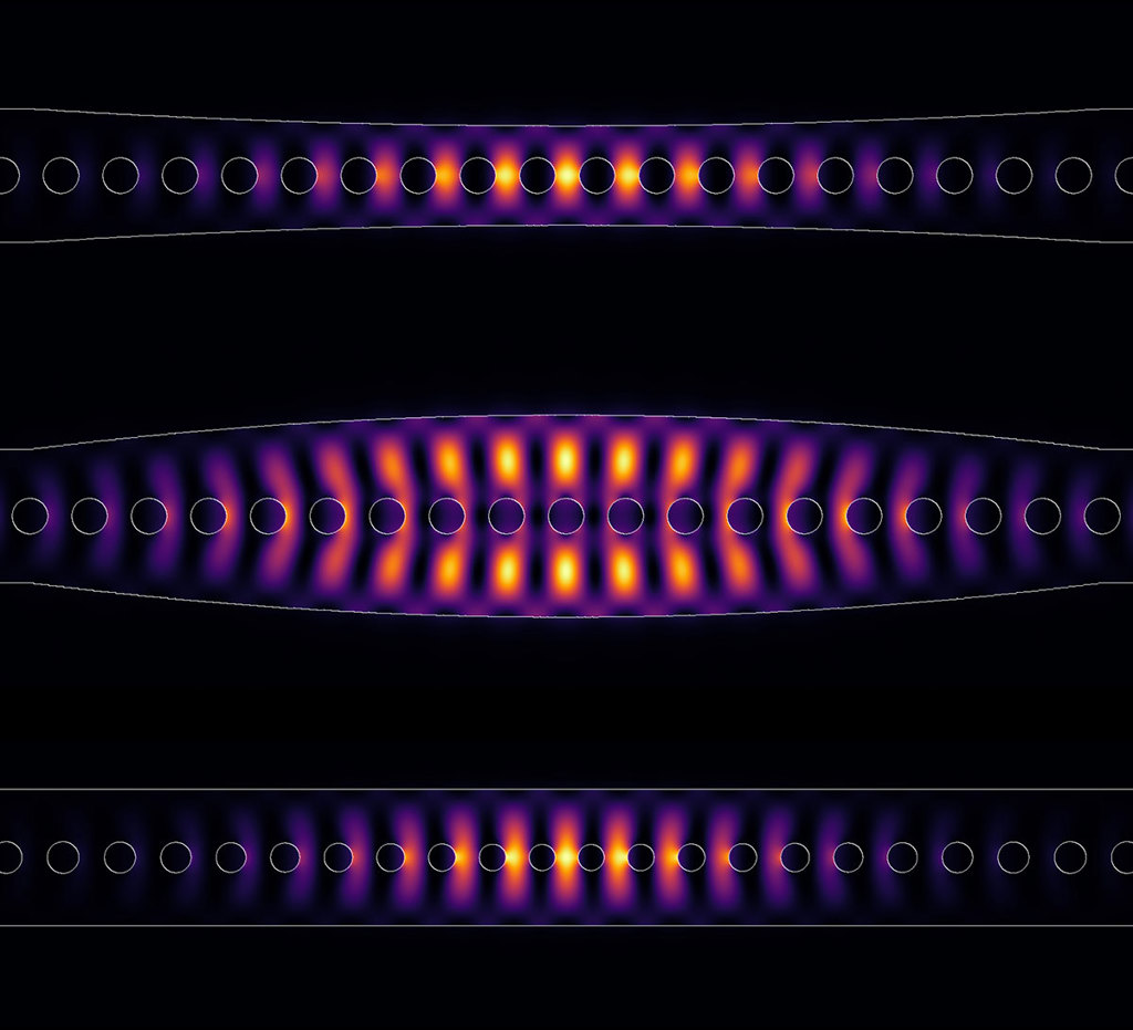
A team at the University of Münster has developed photonic-crystal cavities that could help link up single-photon sources with nanophotonic circuit elements in quantum devices. Three possible photonic-crystal designs, the upper two involving a change in the width of the waveguide and the lower one depending on varying the size and spacing of the holes. [Image: J. Olthaus, P. Schrinner et al., Adv. Quantum Technol.] [Enlarge image]
A major challenge in developing photonic quantum technology is linking sources of single photons with the integrated circuits that will be used to process data. Physicists in Germany have shown how to do this with cavities made from photonic crystals, which could in future be mass-produced using standard semiconductor manufacturing techniques (Adv. Quant. Technol., doi: 10.1002/qute.201900084). The researchers say the cavity design should be flexible enough for use in a broad range of applications, from computing to sensing.
Channeling single photons
Numerous types of single-photon light sources have been developed over the past few decades, from those based on single atoms to others built from carbon nanotubes or tiny pieces of semiconductor known as quantum dots. However, these devices emit in all directions so most of the generated photons that they produce are lost unless those photons can somehow be channeled in space. This can be done on optical benches, but the high vacuums and macroscopic mirrors required for the job make it a labor-intensive and expensive process.
In the latest work, Carsten Schuck and colleagues at the University of Münster instead make cavities from photonic crystals. These artificial structures consist of a transparent dielectric material containing a lattice of air holes that exhibit the photonic equivalent of a semiconductor band gap—a range of frequencies that are blocked by the device.
The idea is to vary either the size and spacing of the holes or the width of the cavity material itself to confine light between the holes. When a single-photon light source is positioned at the very center of such a photonic crystal, the coupling to the cavity’s electromagnetic field can become so strong that photons will be constrained to propagate along the cavity axis.
Designed to scale up
Schuck says that these devices are not designed to have the very high level of control possible by confining single atoms between extremely reflective mirrors. Instead, he says, the aim is to be able to scale up. “The key argument is that nanotechnology allows you to replicate these devices very easily, that if you make one cavity and you make another they are almost identical,” he says. “For us on a chip it practically makes no difference whether we have one device or 10 or 100.”
Group members Doris Reiter and Jan Olthaus, both theorists, used computer simulation to draw up a range of designs, which Schuck and his experimentalist colleague Philipp Schrinner then turned into workable devices using electron beam lithography, fabricating photonic crystals that confine light to within a few hundred nanometers in thin films of silicon nitride. Coupling the cavities to photons from nitrogen–vacancy centers in diamond—at 637 nanometers—the researchers found they got the best results when varying the size and spacing of the holes rather than adjusting the cavity width.
From bridge to street
Schuck points out that cavities with similar quality factors have already been built using photonic crystals. But those cavities, he explains, were free standing—formed by removing the substrate (silicon dioxide) in order to leave a silicon nitride photonic crystal as a bridge surrounded by air. That enhanced the contrast in refractive index between the crystal and its surroundings, improving the device’s performance.
The more elaborate designs in the latest work yield a similar performance even though the photonic crystal is embedded in the substrate—creating what Schuck describes as a “street” rather than a bridge. That, he says, should make it easier to manufacture using standardized fabrication techniques.
“We are thinking in the not-so-far future to have 100 devices integrated into a circuit, with those devices talking to one another,” he says. “The best way to do that is to use CMOS-compatible technology, which means adhering to stricter process standards.”
Toward a reconfigurable circuit
The aim eventually, according to Schuck, is to “build a platform for quantum technology,” a reconfigurable circuit that could be used for multiple applications, including computing, simulation, sensing or communication. However, he admits that some applications are likely to prove harder than others. “If you want to build a quantum computer you need a very high level of control,” he says. “But if you want to produce photons and use them for communication or sensing then we are much closer to doing that.”
Schrinner, on the fabrication side, is currently working to integrate tiny diamond emitters into the photonic-crystal cavities using a novel lithographic technique, says Schuck, having “already seen some coupling” in the new set-up. Theorists Reiter and Olthaus, meanwhile, are studying more complex crystal geometries, including the possibility of using elliptical rather than round holes.