
![]()
[Image: iStock]
The iconic material graphene—atom-thin, 2-D sheets of hexagonally linked carbon atoms—would seem to have everything. It’s 100 times stronger than steel, optically transparent, highly conductive of both heat and electricity, and thin and lightweight enough potentially to provide the foundation for a whole new generation of ultra-slim devices.
The key word, however, is “potentially.” Although graphene was isolated and characterized 15 years ago in Nobel Prize-winning work by Andre Geim and Konstantin Novoselev, and although the intervening decade and a half has seen intensive research work, the material has yet to make its way convincingly into commercial applications.
Two recently published research studies, however, offer a few hints toward ways to make graphene more application-ready. The trick in both efforts? A dose of laser energy.
Lasers tackle graphene’s band-gap envy
The first study, led by researchers at Purdue University and the University of Michigan, USA, and Huazhong University of Science and Technology, China, zeroes in on one of graphene’s biggest shortcomings: it’s lack of an energy band gap (Adv. Mater., doi: 10.1002/adma.201900597). That absence has held back graphene’s use in semiconductor roles in field-effect transistors and other optoelectronic devices. (Some designs, however, have used graphene in the role of a metal in devices, in light of its great electrical conductivity and carrier mobility; see “Optoelectronics in Flatland,” OPN, July/August 2015.)
Researchers have tried a variety of approaches, such as doping with other materials, to coax graphene into showing a band gap, but the resulting gaps have always fallen below 1 eV, limiting potential device performance. Another approach to opening up a band gap is strain engineering—permanently changing the material’s shape. But thus far, strain-engineering efforts have involved simple mechanical stretching, yielding paltry band gaps in the 0.3-0.5-eV area.
Calculations and modeling, however, have indicated that a subtler approach to straining graphene—one that focuses on deforming the material in specific, targeted ways—could bring on substantially wider band gaps. To get there, the U.S.-China team behind the new work turned to a different technique, laser shock imprinting.
Gigapascal-scale shocks
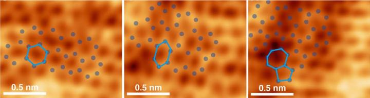
Laser shock imprinting allowed a U.S.-China research team to selectively strain graphene, in ways that increased the material’s band gap from zero to as high as 2.1 eV. [Image: Purdue University/Gary Cheng] [Enlarge image]
In the experiments, the researchers used wet chemical transfer to deposit a sheet of graphene onto an SiO2 mold, lithographically pre-patterned with a structure of nanotrenches, and then covered the graphene with a thin aluminum film. Next, they fired 10-ns pulses from a Q-switched Nd:YAG laser at the target; the laser pulses led to ablation in the aluminum, the strain from which was transduced into the graphene. The short pulse width and tunable power of the laser allowed the team to apply adjustable pressure shocks of tens of gigapascals.
The experiments resulted in sheets of graphene permanently reshaped into a carefully controlled pattern of nanotrenches. In tests of the strained material, the team found that the targeted strain engineering had widened the band gap to values ranging from 1.7 to 2.1 eV, far in excess of earlier efforts, and with no doping or other “extrinsic changes” to the graphene itself. What’s more, the band gap could be tuned between zero and 2.1 eV through variations to laser power and trench geometry.
The Purdue–Michigan–Huazhong researchers believe that the capability for “converting the semimetallic graphene to semiconducting graphene with designed bandgaps” could boost the material’s attractiveness for a range of electronic and optoelectronic applications.
Powering wearable electronics
A second recent study, from scientists at Rice University, USA, brought laser energy to bear in a proof-of-concept for a specific, targeted graphene application: in triboelectric nanogenerators (TENGs) that can harvest energy from body movement to power wearable electronics (ACS Nano, doi: 10.1021/acsnano.9b02596).
TENGs, first demonstrated by the lab of Zhong Lin Wang at the Georgia Institute of Technology in 2012, operate by taking advantage of the triboelectric effect, the same effect that lies behind behind most everyday static electricity. When two materials of the right characteristics—one strongly “tribo-positive” and one strongly “tribo-negative”—are repeatedly pressed together and separated, charge transfer from the tribo-positive to the tribo-negative material builds up a potential difference that can be siphoned off by an attached electrode for power generation.
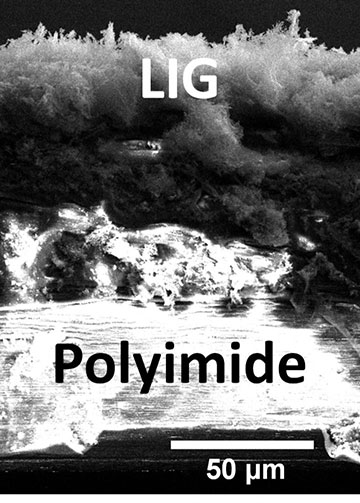
Electron micrograph cross-section of laser-induced graphene/polyimide composite, used by the Rice team to demonstrate a triboelectric nanogenerator. [Image: Tour Group/Rice University]
To make such a system work, the tribo-negative material must lie in close contact both with the tribo-positive one and with a high-conductivity electrode to carry off the output current. And therein lies one problem with these systems: it’s been tough to find a cost-effective way for traditional electrodes, such as precious metals, to be attached snugly to some popular tribo-negative materials such as polyimide. That’s a key issue, as a practical triboelectric nanogenerator to provide power for wearable electronics would need to hold up to many thousands of cycles of mechanical flexing and relaxation.
Laser-induced graphene
The Rice team, led by James Tour, saw a potential solution to the quandary in laser-induced graphene. Specifically, the team began with two carbon-based, strongly tribo-negative materials—natural cork and polyimide—and irradiated them with a 10.6-μm CO2 laser. As work published last year by Tour’s group and others had shown, such irradiation creates a thin graphene foam on the surface of the irradiated material.
The result, in the current case, was composite bilayer films that included both a highly conductive laser-induced graphene electrode and the strongly tribo-negative carbon precursor material (that is, cork or polyimide). The researchers tested the bilayer in triboelectric-generator setups involving a variety of complementary tribo-positive materials, including polyurethane, aluminum and human skin, and were able to generate open-circuit voltages greater than 3.5 kV and peak power exceeding 8 mW. And the system remained stable after 5,000 bending cycles.
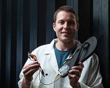
Rice University postdoc and study lead author Michael Stanford, holding a flip-flop with a triboelectric nanogenerator, based on laser-induced graphene, attached to the heel. [Image: Jeff Fitlow/Rice University]
Energy from a flip-flop
The Rice team even embedded one of its laser-induced graphene/polymer TENGs into the sole of a “flip-flop,” the ubiquitous casual footwear, and tied it to a circuit including a capacitor. The repeated contact of the TENG with the wearer’s strongly tribo-positive bare heel allowed the circuit to build up some 0.22 mJ of energy on the capacitor after a 1-km walk.
That rate of energy increase, according to the paper’s lead author, Michael Stanford, is “enough to power wearable sensors and electronics with human movement.”