
![]()
Researchers Ross Hatton, Silvia Varagnolo and Jaemin Lee of the University of Warwick, with a thin patterned metal film created using a new direct-deposition method. The team believes that the technique could help advance the prospects for next-generation, flexible organic solar cells. [Image: University of Warwick]
A key driver of solar-cell research is its potential to offer a credible alternative to fossil fuels, thereby benefiting the environment. But if the clean energy coming from solar cells is environmentally friendly, certain aspects of their production are anything but. One example: the myriad electrodes that must be patterned on the solar-cell surface—usually in processes that require chemical etching or other processes that produce streams of toxic waste.
Now, a team at the University of Warwick, U.K., has come up with what could be a much faster, cheaper and more environmentally sustainable way to directly deposit intricately patterned silver and copper electrodes (Mater. Horiz., doi: 10.1039/C9MH00842J). The researchers believe that the technique, which leverages the well-worn, low-cost method of vacuum evaporation and some clever surface chemistry, is ready for “immediate practical implementation” in a range of applications, present and to come—including the emerging new generation of thin-film, flexible solar cells, next-generation sensors and low-emissivity glass.
Nasty chemicals
The patterned electrodes on the surface of solar cells, as well as other optoelectronic devices such as plasmonic sensors, can be quite intricate, involving arrays of structures on the micron scale or even smaller. The usual method for making these structures involves putting down a continuous layer of copper or silver (the two most common electrode metals), and then etching away the parts where the metal isn’t needed using some rather nasty chemicals—a process that creates streams of toxic chemical and metal waste.
A better method would be to directly deposit the metals selectively in the desired pattern, reducing waste and materials costs. But the most common way of doing this, electrochemical deposition, is also, in the words of the researchers behind the new study, “an inherently chemical intensive and slow solution based process.”
Non-stick surface
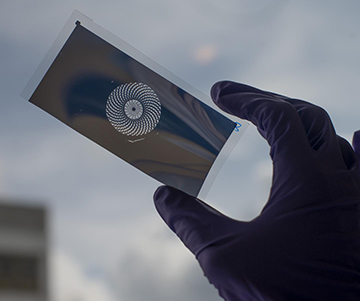
A patterned metal made using the new technique. [Image: University of Warwick]
Instead, the Warwick team, including chemists Silvia Varagnolo, Jaemin Lee and Ross Hatton and physicist Houari Amarib, looked at the prospects for creating patterned electrodes using a well-established, low-cost manufacturing method, simple vacuum (thermal) evaporation, widespread in the food-packaging industry and in research labs as well. The tough bit, however, was trying to figure out how to adapt this technique, used for the creation of large-area metal films, to create the highly patterned, semi-transparent and ultrathin electrodes used in solar cells and optoelectronic devices.
The team found that the secret to doing so lay in an intermediate material—a 10-nm-thick patterned thin film of a cheap, low-toxicity organofluorine, FTS, that can be printed onto the device surface. Once that film is in place, it turns out that silver or copper, deposited using vacuum evaporation, will not condense onto the parts of surface covered by the FTS film, but only on the bare parts. (Interestingly, and maybe not coincidentally, organofluorine compounds such as FTS are also common as an ingredient in non-stick cooking pans.) Thus the metal goes only where the pattern design requires it, with no need for chemically etching away parts of a continuous metal surface to create the final electrode pattern.
Six million holes per square centimeter
As a proof of concept, the team used micro-contact printing of FTS to fashion templates for a variety of patterned electrodes, and created prototype devices—including semitransparent organic solar cells with a top silver electrode that packed in six million 2-μm-diameter apertures, or holes, per square centimeter. “To our knowledge,” the team writes, such a feat “cannot be achieved by any other scalable means directly on an organic electronic device.”
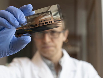
Team leader Ross Hatton, with a sample of patterned metal created via the Warwick team’s direct-deposition method. [Image: University of Warwick]
While the researchers used micro-contact printing for the prototype, they stress that they “see no insurmountable obstacle” to scaling up to low-cost, industrial-scale methods such as continuous roll-to-roll processing of the organofluorine layer, and thereby to applying the technique to create patterned metal films on an industrial scale. And the technique involves no metal removal, and thus no metal and toxic chemical wastes, which the team argues gives it an edge in materials costs and environmental sustainability.
The team believes that the technique—which, the researchers maintain, should be ready for “immediate practical application” in light of the work already done—could come in particularly handy in creating the next generation of lightweight, bendable thin-film perovskite or organic solar cells. Hatton, the team leader, said in a press release that the team’s innovation “enables us to realize the dream of truly flexible, transparent electrodes matched to needs of the emerging generation of thin-film solar cells, as well as having numerous other potential applications ranging from sensors to low-emissivity glass.”