
![]()
Two research groups have reported progress on efficiently harvesting 2-D materials, and on creating better heterostructures of them for optoelectronic applications. [Image: Massachusetts Institute of Technology/Peng Lin]
Since the first isolation of graphene in the laboratory some 15 years ago, researchers have spun big dreams about the application of it and other atomically thin, “2-D” materials, such as transition-metal dichalcogenides (TMDs), to create ultra-strong, lightweight and flexible devices.
But achieving those dreams of hyper-thin, flexible screens and bendable mobile phones will involve practical schemes to create well-behaved stacks, or heterostructures, of such 2-D semiconductor materials to achieve specific optoelectronic effects. And it will require ways to produce those stacked structures at the scale not of tiny flakes in the lab, but of semiconductor wafers on the production line.
Several labs have recently reported interesting progress toward the goal of such scalable, ultra-thin heterostructures. In one case, a research team in China, Australia and the United States fashioned atomically thin heterostructures consisting of monolayers of a 2-D TMD, molybdenum diselenide (MoSe2), and an organic material, and found that the organic–inorganic hybrid showed dramatic increases in photoexcitation efficiency and photoluminescence (Adv. Mater., doi: 10.1002/adma.201803986). And in separate work, researchers in the United States and Korea developed a method that they say could allow the reliable creation of high-quality TMD monolayers, and heterostructures of the same, at a wafer scale (Science, doi: 10.1126/science.aat8126).
Making excitons mobile
Among 2-D materials, TMDs—which combine a transition metal such as tungsten or molybdenum with a chalcogen such as sulfur or selenium—hold particular interest for optical engineers, owing to the large indirect band gap of these materials. That could make them a great component for photodetectors, LEDs and solar cells, for example (see “Optoelectronics in Flatland,” OPN, July/August 2015). Recent work by researchers from Nanjing University, China, the Australian National University (AMU), and the University of Wisconsin, USA has focused on how to beef up the light–matter interactions in monolayer TMDs.
One way to engineer such interactions is to pair those inorganic 2-D materials up with organic molecular semiconductors. Such an organic–inorganic pairing, previous work had suggested, can increase the mobility of excited electron–hole pairs—so-called excitons—across the heterostructure interface. And that, in turn, could boost the semiconductor stack’s efficiency in converting light to electricity (in applications such as photodetectors and photovoltaics) and electricity into light (in LEDs).
The problem, the Nanjing-AMU-Wisconsin team points out, is that this previous work has integrated 2-D TMDs with bulk organic materials (with a thickness of greater than 20 nm). That’s insufficient, the researchers suggest, for the atom-by-atom control required to optimize light–matter interactions in these structures. And it also takes away some of the potential to integrate these heterostructures into exotic, ultra-thin devices such as bendable phones.
Lighting up MoSe2
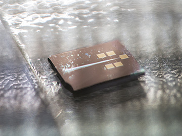
The semiconductor heterostructure developed by the Nanjing-ANU-Wisconsin group is not visible to the naked eye, but sits between gold electrodes on the pictured chip, which is roughly 1 cm square. [Image: Jack Fox, ANU]
To get to true atomically thin TMD–organic heterostructures, the researchers built on previous work studying organic semiconductors only a few molecular layers thick (Phys. Rev. Lett., doi: 10.1103/PhysRevLett.116.016602). With that work as a foundation, they used physical vapor deposition to put down an ultra-thin, 2-D layer of an organic semiconducting material, pentacene, on top of a boron nitride film a few atomic layers thick. They then completed the heterostructure by depositing dry flakes of MoSe2 on top of the organic layer. Finally, they attached some gold electrodes to put the structure through its optoelectronic paces.
The team found that these 2-D pentacene-MoSe2 heterostructures showed a so-called type-I band alignment. In this case, that alignment meant that excitons could be pumped across the organic–inorganic heterostructure interface more than 86 times more efficiently than for photoexcitation in MoSe2 alone. And that exciton-pumping efficiency showed up clearly in characteristics such as strongly enhanced photoluminescence in the MoSe2 layer.
All of that, according to members of the research team, could ultimately play out in devices that are both optically bright and have some exotic properties. “The light emission from our semiconducting structure is very sharp, so it can be used for high-resolution displays,” said ANU Ph.D. researcher Ankur Sharma in a press release. “And, since the materials are ultra-thin, they have the flexibility to be made into bendable screens and mobile phones.” More broadly, the study concludes that the work provides “a new way to engineer the light–matter interactions in atomically thin semiconductors and their hybrids, enabling various new optoelectronic devices, such as ultrathin lighting diodes, heterostructure lasers, etc.”
Beyond the “adhesive tape” method
The work reported by the Nanjing-ANU-Wisconsin team offers a nice win for the optoelectronic potential of 2-D semiconductor heterostructures. But how the inorganic part of those structures was made—laborious mechanical exfoliation of MoSe2 flakes—remains a problem for scaling such structures up to commercial use. Separate work by another team could offer a way to build up TMDs heterostructures on a scale compatible with semiconductor wafer production.
Even a decade and a half after graphene’s discovery, labs are still making 2-D inorganic materials in much the same way they did in 2003: the “adhesive tape” method, which involves using a sticky tape to peel flakes of the 2-D material off of a bulk material, and then assembling those flakes into films one or several atomic layers thick. It’s a time-consuming and imperfect process at best, requiring many hours to assemble a single device in the lab.
Divide and conquer
To get past that roadblock to commercialization, researchers at the Massachusetts Institute of Technology (MIT), Georgia Tech, the University of Virginia and the University of Notre Dame, USA, and Yonsei University, South Korea, looked at a very different approach, which the team believes could allow routine wafer-scale integration of 2-D materials.
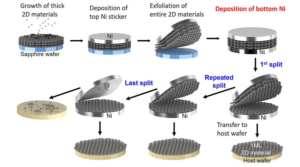
A schematic illustration of the layer-resolved splitting method, which can create wafer-scale monoatomic layers of some 2-D materials. [Image: Massachusetts Institute of Technology/courtesy of the researchers] [Enlarge image]
The technique, which the team calls layer-resolved splitting, involves first growing a relatively thick stack of the 2-D TMD material, around 5 cm in diameter and multiple atomic layers thick, on top of a sapphire wafer. Then, a 600-nm-thick film of nickel, which adheres strongly to the 2-D TMD, is applied to the top of the stack, and bent back to mechanically release the 2-D material from the sapphire substrate.
Next, a second nickel layer is added to the bottom of the stack. As the top layer is once again bent back, crack propagation across the stacked TMD material and then along the interface between the atomically thick monolayers allows the monolayers to be peeled off one by one and attached in a single large piece, rather than a mosaic of exfoliated flakes, to a new wafer substrate.
Toward high-throughput manufacture
The team was able to use the technique to create 5-cm-diameter monolayers of wafer-scale uniformity from a variety of TMDs, including MoSe2, MoS2, WSe2, and WS2—and to do so in a matter of minutes, compared with the hours required to build up high-quality layers using the adhesive-tape method. What’s more, they showed that the 2-D layers created in this way could be efficiently stacked up into a variety of heterostructures and even arrays of heterostructures with enhanced optoelectronic properties, through a method they dubbed quasi-dry stacking.
The team believes that the layer-resolved splitting technique could offer a key to high-throughput manufacturing of TMD-based heterostructures—and, thus, “a stepping stone” toward the commercialization of devices based on such structures. “All you need to do is grow these thick 2-D materials, then isolate them in monolayers and stack them up,” noted team leader Jeehwan Kim of MIT. “So it is extremely cheap—much cheaper than the existing semiconductor process. This means it will bring laboratory-level 2-D materials into manufacturing for commercialization.”