
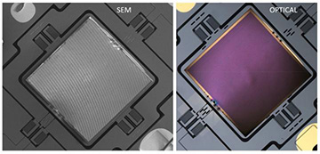
Scanning electron micrograph (left) and optical microscope image (right) of metalens-on-MEMS device developed by Harvard-Argonne research team. [Image: Center for Nanoscale Materials, Argonne National Lab]
Recent years have seen an explosion of research in flat optical components fashioned with so-called metasurfaces—intricately engineered, planar configurations of subwavelength elements. But most of these flat optical elements have lacked a means of active control, a drawback that’s held back their use in many applications.
Research groups at Harvard University and the Argonne National Laboratory, USA, have now teamed up to create a dynamic metasurface lens, by marrying the metalens with an electrically controllable microelectromechanical system (MEMS) mirror (APL Photon., doi: 10.1063/1.5018865). The team believes that the proof-of-concept device could lead to ultrathin controllable optical systems with a range of applications in imaging, projection, lidar and more.
Meta + MEMS
Metalenses and other metasurface optical elements consist of arrays of subwavelength metallic or dielectric, phase-shifting structures, so arranged to match the phase-shifting behavior of more conventional, bulk optics such as lenses. Research in these exotic surfaces has led to a range of designs for lightweight, flat lenses, polarimeters and other optics. But there’s been a catch—most of these devices have been static, which has limited their use applications involving beam steering, scanning and other dynamic functions.
To get to a controllable metalens, the lab of Federico Capasso at Harvard, a leading group in metalens and metasurface engineering, joined forces with that of Daniel Lopez at Argonne, an early developer of MEMS systems. The device that the team has demonstrated—900 microns across and only 10 microns thick—uses a MEMS-driven mirror to reflect a scanned infrared beam, which is then focused by an ultrathin metalens. The MEMS scanner, actuated by tiny electrostatic vertical comb drives, can rapidly vary the angle of the lens on two axes by as much as 9 degrees, allowing for dynamic beam steering by the device.
Platinum glue
The device begins with a plasmonic metasurface lens, comprising an array of 50-nm-thick gold disks ranging from 1.2 to 2 microns in diameter, sitting atop a 400-nm-thick SiO2 layer and a 200-nm-thick layer of gold film. The researchers used standard photolithography techniques to fabricate the reflective lens on a silicon-on-insulator wafer. They then employed a focused-ion-beam tool, integrated with a micromanipulator needle, to cut the lens to size, ease it into position on top of the MEMS platform, and glue it into place with tiny blobs of platinum. The team notes that this simple “welding” approach to the device’s construction allows for the integration of hybrid structures built with a range of different processes.
To test the metalens-MEMS device, the team shone a 4.6-μm quantum cascade laser on the device. The researchers then compared the optical profile of the reflected light focused by the metalens, as the lens-on-MEMS device was rotated at various increments, with numerically simulated profiles. They found that, for small rotations (up to 2.5 degrees), tilting the lens preserved “the focused beam profile in general,” and also preserved the measured full-width half-maximum (FWHM).
Expanding applications
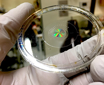
Capasso's lab has also been experimenting with metalenses controlled by “artificial muscles,” made of an electrically actuated elastomer from soft-robotics research. [Image: Harvard SEAS]
While the device represents only a proof of concept limited to the mid-infrared, the researchers believe that it can ultimately be extended to visible light and other parts of the spectrum, and that marrying the metalenses with more complex MEMS design could expand the system’s flexibility. As those improvements come to pass, the team envisions applications in MEMS-based microscope systems, compact lidars for autonomous vehicles, projection imaging, and even new kinds of reconfigurable, fast spatial-light modulators. Co-team-leader Lopez argues that the extreme miniaturization, coupled with the use of CMOS-friendly manufacturing for all components, could ultimately bring complex optical devices “as thin as credit cards.”
Capasso’s lab is exploring other methods for dynamically shaped metalenses as well. In another recent paper (Sci. Adv., doi: 10.1063/10.1126/sciadv.aap9957), the team at Harvard tied a large-area metalens to dielectric elastomer actuators—a material from soft-robotics research sometimes referred to as “artificial muscles”—and used the electrically actuated elastomers to control the lens focal length and to correct for astigmatism and image shift.