
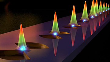
In the work led by Sharon Weiss at Vanderbilt University, a linear photonic crystal consists of bowtie-shaped holes that confine light in time, and nanoscale bars connecting the bowtie lobes that act as funnels for subwavelength confinement of optical energy in space. [Image: Ella Maru Studio]
A team led by OSA Fellow Sharon Weiss of Vanderbilt University, USA, has demonstrated an all-dielectric “bowtie” structure that combines the tight spatial light confinement of plasmonic resonators with the ultralow losses and long cavity lifetimes of photonic crystals (Sci. Adv., doi: 10.1126/sciadv.aat2355). The demo—which physically realizes theoretical work highlighted in OPN’s 2017 Year in Optics roundup—could, according to the researchers, create opportunities for harnessing extremely strong light–matter interactions in applications ranging from computing to quantum optics.
Questions of confinement
A long-standing conundrum of nanophotonics has been how to achieve deep-subwavelength light confinement (measured by a parameter called the mode volume, Vm) while holding the light in place in a cavity for long periods (an ability characterized by the cavity’s quality factor, Q). Plasmonics—the enhancement of optical fields at metal-dielectric interfaces, using nanoscale metallic resonators or antennas—can give you very tight spatial confinement (low Vm). But plasmonic devices tend to be lossy, with anemic Q factors, and thus the spatially confined light energy quickly dissipates.
More recently, work leveraging Mie resonances with high-index nanoparticles has shown the ability to achieve plasmonic-style subwavelength localization in low-loss dielectrics, for a potential end run around plasmonics’ loss problems. But even there, according to Weiss, the problem of confinement in time as well as in space remains. “If you have an individual Mie scatterer, you don’t have a cavity,” she says. “You can’t have a resonant mode that’s trapped in a cavity that has a long lifetime.”
Enter photonic crystals
In a theoretical study in late 2016, Weiss, along with OSA member and then-grad-student Shuren Hu (now with the semiconductor fabrication firm GlobalFoundries), proposed an answer: combine the subwavelength-confinement properties of nanoscale dielectrics with the near-legendary Q values of photonic-crystal cavities (ACS Photon., doi: 10.1021/acsphotonics.6b00219).
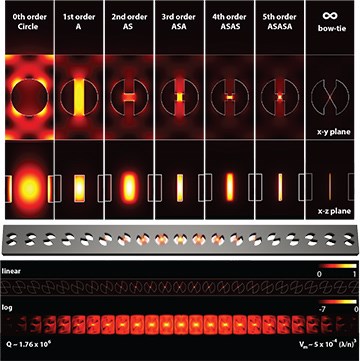
Theoretical work in late 2016 by Weiss and then-grad-student Shuren Hu showed that bowtie nanostructures could combine small mode volumes with high quality factors, achieving both spatial and temporal confinement. [Image: S. Hu and S. Weiss, Opt. Photon. News, December 2017]
In a series of elegant numerical simulations, Hu and Weiss applied specific boundary conditions and the foundational mathematics of electromagnetism, Maxwell’s equations, to a photonic-crystal structure. They showed that by modifying the circular air hole of a typical photonic crystal into a bowtie shape, and tying the two bowtie lobes together with a subwavelength dielectric bar, they could, in principle, approach both the tiny mode volumes of plasmonics and the lofty quality factors of photonic crystals.
The process works in two steps. Incident light becomes localized in the photonic-crystal cavity air hole. Then, the cavity’s bowtie geometry, and the energy concentration at the bowtie tips, funnels and squeezes the optical energy into the nanoscale dielectric bar. The result is deep subwavelength confinement of the light energy, combined with the photonic crystal’s long cavity lifetime. “We kind of take the best of both worlds,” says Weiss. “We put this subwavelength scatterer within a cavity environment.”
Yes … but can you make it?
Elegant as the theory was, realizing it in the physical world took considerable work. “A lot of the reviewer comments that came back from the theory paper were, We don’t believe that you can actually fabricate it,” says Hu. “The theory is wonderful, but can you really demonstrate it?”
A particular challenge, he notes, lies in the sharp angles and 10-nm length scale of the nano-bowtie features. Given the strong optical field at the angles of the bowtie, where energy is funneled from the air mode of the photonic-crystal cavity into the dielectric scatterer, the structure becomes very sensitive to even the tiniest fabrication defects. “How to consistently define the shape—not just in one bowtie, but in a periodic structure, because it’s a photonic crystal—that’s the biggest challenge,” according to Hu.
To meet that challenge, Hu and Weiss teamed up with the silicon-photonics group of OSA Senior Member William Green at the IBM T.J. Watson Research Center, USA. Hu spent seven months working with the IBM unit to fabricate the theoretically modeled structure. The team did additional numerical work to further flesh out the structure; used electron-beam lithography to fashion the device on silicon-on-insulator wafers; and then tweaked and biased the parameters of each iteration of fabricated crystals to tune the critical properties. There was, Hu says, “a lot of trial and error.”
Deep-subwavelength confinement in silicon
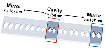
[Image: S. Hu et al., Sci. Adv. 4, eaat2355 (2018); doi: 10.1126/sciadv.aat2355 (CC BY-NC)]
The result was a silicon photonic-crystal cavity consisting of unit-cell bowties with a radius of 150 nm, and with mirror unit cells of 187 nm radii on either end, arrayed in a 700-nm-wide waveguide. To put the structure through its paces, the team tied it, via lensed optical fiber, to a 1500-to-1630-nm tunable continuous-wave laser, and measured the field distribution using near-field scanning optical microscopy.
Hu and Weiss found that the fabricated structure did indeed link up spatial confinement with temporal confinement. The quality factor, on the order of Q = 105, was, Weiss says, “commensurate with some of the best photonic crystals.” And the mode volumes, on the order of 10–3 to 10–4 times the cube of the wavelength, were within a factor of two of the Vm for similar plasmonic structures.
Scaling up toward applications
Weiss also points out that, unlike some other efforts that attempt to confine light in photonic-crystal cavities, the light in their device is trapped not in air but in the silicon itself. That should be a big plus, she reckons, in moving the design into real applications that take advantage of silicon’s material properties and nonlinearities.
Sharon Weiss and Shuren Hu. [Images: Vanderbilt University/Shuren Hu]
Among those applications, Weiss believes that those most in reach in the near term involve efforts to leverage silicon photonics in microelectronics and computing. There, she suggests, the ability to amplify a small amount of light in a resonant silicon-based cavity, with low losses, could provide more bang for a given energy input, and thus possibly reduce power requirements.
Hu adds that even more exotic applications, envisioned in some recent theoretical studies, could come to fruition—such as using the bowtie structures in optical fiber to achieve super-resolution imaging, or designing structures that can achieve nonlinear effects with a single photon. “It’s basically opened up a lot of possibilities for manipulation of light at the nanoscale without losing the Q factor,” he says. “That’s what I’m really excited about.”
Realizing those possibilities will take a significant amount of work to scale up from these initial experiments, and to reproducibly create the exquisitely precise photonic-crystal structures required. Hu, at GlobalFoundries, is now co-P.I. with Weiss on a new project, funded by a U.S. National Science Foundation GOALI (Grant Opportunities for Academic Liaison with Industry) award, to work toward scale-up and proof-of-concept applications. Weiss notes that Hu began the work as a grad student in her lab under another GOALI grant, with IBM. “So it kind of comes full circle,” she says. “Which is also a nice story.”