
[Image: Courtesy of Onur Tokel, Bilkent University]
For decades, the information technology revolution has literally been written on the surface of silicon chips, where lithography at ever finer scales has enabled the rapid advances in device complexity and speed summed up in Moore’s law. But what about the possibilities for electronic and photonic structures and devices inside the silicon wafer?
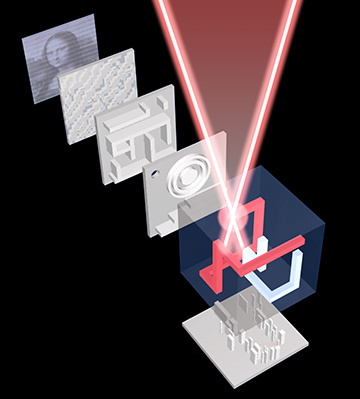
A team led by researchers at Bilkent University and the Middle East Technical University in Ankara, Turkey, now offers an answer. The team has developed an approach that uses a combination of direct infrared laser writing and optional chemical etching to pack 3-D microstructures and photonic devices deep inside bulk silicon, while leaving the top and bottom surfaces unmolested (Nat. Photon., doi: 10.1038/s41566-017-0004-4). The researchers report that they’ve used the technique to fashion a variety of “in-chip” microstructures including microfluidic cooling conduits, lenses, holograms, and other photonic devices “that match or surpass corresponding state-of-the-art device performances.”
Exploiting nonlinear feedbacks
The idea of “3-D silicon devices” is hardly a new one. In the past, for example, researchers have exploited vertical stacks of planar silicon structures to fashion waveguides, microrings and other silicon-photonic devices in 3-D (Opt. Express, doi: 10.1364/OE.19.017758). But these techniques relied on building up and fusing silicon layer by layer rather than writing structures directly into the bulk material. Around a dozen years ago, another group succeeded in creating optical waveguides directly inside crystalline silicon using femtosecond laser pulses (Opt. Lett., doi: 10.1364/OL.30.000964). According to the Turkish team, however, early efforts such as this at direct 3-D writing in silicon tended to be limited to structures near surfaces or interfaces, and couldn’t carve structures inside silicon at arbitrary depths.
The Turkish team, led by Onur Tokel of Bilkent University, dug deeper into bulk silicon through a setup that begins with a custom-built nanosecond pulsed fiber laser, with a center frequency of 1.55 microns. Silicon is transparent to light at these infrared wavelengths, which allows the beam to penetrate beneath the surface of the chip.
Then, using a 40× microscope objective, the researchers focus the beam beneath the silicon surface, and trigger a variety of nonlinear feedback mechanisms involving the interaction of the silicon with the incident beam and counterpropagating infrared light reflecting from the back surface. These interactions lead to self-focusing and collapse of the beam (attributable to thermal lensing) at a controllable location deep within the silicon block. The beam collapse, in turn, permanently modifies the crystal structure and refractive index within a roughly 1-micron spherical volume around the collapse zone.
Speeding up the process
In principle, the technique allows the researchers to move from point to point in the chip, building the in-chip structures sequentially—one pulse at a time. But there’s the rub: According to Tokel’s team, creating devices on cubic-millimeter scales using such point-to-point processing can require between 100 million and 10 billion separate beam-positioning steps. That would make actual use of the technique a practical impossibility, even with the fastest beam-positioning equipment currently in use.
To get past that time sink, Tokel and colleagues exploited a nice embedded trick in the technique. It turns out that the same nonlinear feedback effects that allow the point-scale modifications beneath the chip surface also promote the growth of self-organized, rod-like structures in the direction of beam propagation. These rodlike structures, according to the team, can be used as controllable building blocks that require only the application of additional laser pulses, without beam repositioning, and that can be tied together selectively with point-to-point processing to create finer features. Using the building-block approach, the team reports, “the fabrication time is reduced from thousands of hours to mere minutes.”
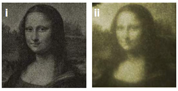
Devices demonstrated in the work included an experimental realization of a 600×600-px digital hologram of the Mona Lisa (left) in silicon (right). [Image: Courtesy of Onur Tokel, Bilkent University]
Holograms, channels and microstructures
Tokel’s team also found that it could apply selective chemical etching to the laser-modified areas to allow 3-D sculpting of the entire wafer. Using the combination of nonlinear laser writing and optional chemical etching, the team was able to demonstrate in-silicon holograms, information-storage structures analogous to barcodes, microchannels that could be used (for example) for chip cooling, in-chip waveguides, and a variety of other microstructures.
In addition to scientists from the Turkish institutions, the work also included contributions from researchers at the Institute of Ion Beam Physics and Materials Research, Dresden, Germany, and the Massachusetts Institute of Technology and Harvard Medical School, USA.