
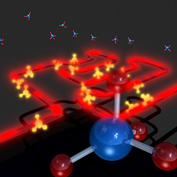
In IBM’s silicon photonics absorption spectrometer, the portion of infrared light protruding outside the waveguide is absorbed by methane molecules, enabling spectroscopic measurement of the methane concentration. [Image: Joe Green, Beaverworks Canada]
Scientists need to detect trace gases for a variety of reasons: monitoring greenhouse-gas levels in remote locations, for example, or sensing natural-gas leaks in cities. Using silicon photonics technology, a U.S. research laboratory has created a tiny near-infrared spectrometer with a nose for methane (Optica, doi:10.1364/OPTICA.4.001322).
Spectral fingerprints
Infrared-tunable diode laser absorption spectroscopy (IR-TDLAS) has already proven its ability to detect the spectral fingerprint of methane, which is both a critical greenhouse gas and the main component of natural gas, at parts-per-trillion concentrations by volume. The units currently available for performing this kind of spectroscopy in the field, however, require mobile or handheld setups that do not lend themselves to continuous, remote monitoring.
William M.J. Green and his colleagues at IBM Corp.’s Thomas J. Watson Research Center, N.Y., USA, built an infrared spectrometer in a silicon-on-insulator package just 16 mm2 in surface area. Despite that small size, the device contains a 10-cm-long, 430-nm-wide silicon waveguide, with an input beam from a laser operating at 1650-nm wavelength—a prominent feature in the absorption spectrum of methane.
To test the tiny spectrometer, the researchers ran it side-by-side with an open-path, free-space methane sensor in an environmental chamber. They split the beam from a distributed-feedback laser and sent it through both systems. During a test with rising levels of methane inside the chamber, the chip-based spectrometer matched the free-space sensor’s detection of the environmental change. The silicon-waveguide device was limited only by Gaussian noise and reached a detection limit of about 20 parts per million after 1,000 seconds of observing time.
No moving parts
The chip-scale spectrometer has no moving parts and could be manufactured through conventional complementary metal-oxide-semiconductor (CMOS) techniques such as deep-ultraviolet photolithography. According to the researchers, thousands of these tiny detectors could be made from a single semiconductor wafer, which would significantly lower their manufacturing cost and their integration into low-power remote-monitoring platforms.