
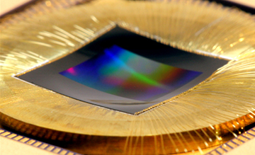
Researchers from Microsoft Corp. and HRL Laboratories created a process to deform standard, flat CMOS sensors into highly curved imaging surfaces. The curved sensors maintain high pixel counts, and allow better sharpness and illumination consistency in captured image. [Image: Guenter et al., Opt. Express, doi: 10.1364/OE.25.013010]
Researchers from Microsoft Corp. and HRL Laboratories, USA, have developed a method for deforming a standard commercial CMOS image sensor into a highly curved shape that’s more compatible with the image actually formed by a camera lens (Opt. Express, doi: 10.1364/OE.25.013010). The team reports that its curved sensor, coupled with a custom-designed lens matched to the sensor’s curvature, can create images superior in sharpness and illumination consistency to analogous flat-sensor cameras—while reducing the need for some of the aberration-correcting optical elements required by flat sensors.
The eyeball model
To grasp the rationale for a curved image sensor, one need only think of the shape of the human eye, in which a simple, compact lens casts an image onto a curved retinal surface. Indeed, it’s been known for nearly two centuries that thick-lens optical systems naturally focus their object plane onto a curved image surface (with the curvature radius of the focusing surface determined by the specifics of the lens). A lack of curved imaging surfaces suitable for mass production, however, has made it complicated to put that knowledge to practical use.
Instead, conventional cameras use flat imaging surfaces (such as CMOS image sensors), and rely on additional optical elements to flatten the field of view and correct for spherical aberration. Recent work has suggested that, by reducing the requirement for these additional optics, a curved imaging surface could produce a sevenfold reduction in length and perhaps a 37-fold reduction in weight—while substantially improving modulation transfer function and illumination consistency in the imaging package. But today’s CMOS imaging sensors comprise high-density pixel arrays embodied on flat, highly stiff silicon slabs, which are difficult to curve without substantially degrading the image quality.
The Microsoft-HRL team attacked that problem by first carefully studying the evolving stress-strain state of bending silicon, and then equally carefully tuning a bending process to minimize harmful tensile strains and instabilities. The group’s process begins with a thinned commercial CMOS sensor, which is placed in a specially constructed mold and undergoes gradual pneumatic pressure to reshape the sensor according to the contours of the curved mold. By keeping the process gradual and by allowing the edges of the silicon die to float freely rather than fixing them, the process allows tensile stresses to dissipate and leads to a smooth, curved sensor surface.
Camera test
The researchers found that the process allowed the creation of image sensors with more than twice the curvature allowed by previous bending methods—and with no degradation of imaging quality. Moreover, the availability of a curved imaging surface opens up the lens design space, according to the team, which designed a custom, fast (f/1.2) lens matched to one of its curved sensors, and then tricked out a prototype camera with the setup. The prototype camera was able to achieve “exceptional resolution of 3220 line-widths per picture height … and nearly 100 percent relative illumination across the field,” a performance superior to that of a high-end professional flat-sensor camera using a 50-mm f/1.2 lens.
The researchers believe that the combination of a curved imaging plane and the clever, compact new lens designs enabled by it could open up applications in handheld devices, head-mounted displays, surveillance imaging and more. And the use of commercial silicon sensors as the raw material suggests the ability to scale up the process of creating curved sensors in the context of existing CMOS manufacturing. “We showed that you can take an off-the-shelf sensor, curve it and dramatically improve the performance of the optical system,” the paper’s lead author, Brian Guenter, said in a press release. “This can be done with relatively low costs and effectively no downside.”