
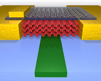
The high-performance photodetector created by the Minnesota team uses few-layer black phosphorus (red atoms) to sense light in the waveguide (green material). Graphene (gray atoms) is used as a top gate to tune the performance. [Image: University of Minnesota, College of Science and Engineering]
Much of the excitement surrounding electronic and photonic applications of 2-D materials has centered on graphene, atom-thick layers of carbon with an array of striking properties. But other varieties of 2-D materials with different strengths are also drawing attention. A team of scientists from the University of Minnesota (USA) has now shown that one such material—layered black phosphorous—could shine as a photodetector element in integrated photonic circuits (Nat. Photon., doi: 10.1038/nphoton.2015.23).
While graphene has a variety of characteristics, such as saturable absorption, that have made it a focus of effort and study in optoelectronics research, one disadvantage of the material for photodetection is its lack of a band gap. As a result, although graphene has been used as a component in wideband photodetectors, those detectors tend to have a very large “dark current” (the residual current flowing in the material in the absence of incident light). Thus graphene photodetectors have relatively high noise floors and levels of electrical leakage.
Black phosphorous—with a band gap of 1.8–2.0 eV in monolayers, which can be narrowed to as little as 0.3 eV by stacking individual layers—has the potential for much higher efficiency in photodetection. And given the ultrathin, 2-D geometry of the black phosphorous layers, “it makes perfect sense to place them on chips with flat optical integrated circuits,” notes Mo Li, the leader of the Minnesota research team.
The scientists demonstrated the potential of the material in silicon photonics by constructing a field-effect transistor (FET) consisting of around 20 black phosphorous monolayers. That thickness tuned the material’s band gap to the near-infrared, telecom band, according to the researchers. They then integrated the black phosphorous FET into a silicon photonic waveguide and capped the device with a few-layer-thick film of graphene, to act as a top gate. The result was a gated photodetector integrated within the waveguide, with a very low dark current, high sensitivity in the near infrared, and a very high response rate.
The team concludes that “In nearly every aspect of their performance, [black phosphorous] photodetectors can outperform graphene photodetectors and are more realistic for practical use.” The researchers see considerable potential for black phosphorous as a linchpin component in integrated optical communications, enabling both high-sensitivity detection and also, potentially, generation of light in the same circuits, and helping to enable on-chip communication using light. “This could have huge potential for high-speed communication between CPU cores,” says lead author Nathan Youngblood, “which is a bottleneck in the computing industry right now.”