
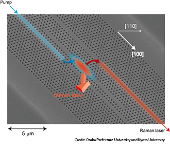
Depiction of the Raman laser action in the device design.
Researchers at two Japanese universities have taken another step in the ongoing quest for silicon-based lasers that can operate on the tiny scale of modern electronic circuitry. The team recently built an optically pumped Raman silicon laser with a cavity less than 10 µm across (Nature 498, 470).
The “silicon laser” has been the goal of scientists who wish to integrate photonics with existing electronic technology. With four electrons in its outer shell, silicon has an indirect bandgap that makes it inefficient at amplifying light without a little nano-engineering.
The group, led by Yasushi Takahashi of Osaka Prefecture University and Susumu Noda of Kyoto University, built the cavity of their tiny laser out of a photonic crystal with a triangular lattice structure formed by circular holes (roughly 100 nm in diameter) in silicon. They pumped it with a laser beam at 1,428 nm, resulting in Raman scattering with a Raman-Stokes frequency of 1,543 nm—right in the telecommunications band. The cavity was designed with a resonance frequency to coincide with that Raman-Stokes frequency, resulting in continuous-wave laser action.
Previously reported Raman silicon lasers have been roughly three orders of magnitude larger in size and required several tens of milliwatts of pump power to operate. By contrast, the Takahashi-Noda team’s device has a lasing threshold of 1 microwatt.
The researchers would like to reduce the threshold pump power below 100 nanowatts, perhaps to the point where a tiny electrical signal could create enough spontaneous emission to trigger the laser. Then, modulation of the signal at telecom rates could boost plans to put tiny silicon lasers into integrated circuits.