
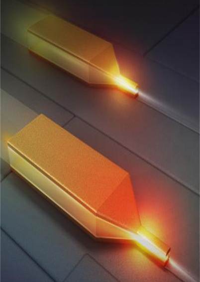
Illustration of a device that can focus near-infrared light into a point just a few nanometers across. Credit: Young-Hee Lee, Caltech.
Squeezing light down to the smallest possible space is a crucial consideration when integrating tiny devices onto a single photonic chip. Scientists in California (U.S.A.) have built a tiny plasmonic waveguide that “nanofocuses” near-infrared light to a point less than 100 nm wide (Nature Photon., doi: 10.1038/nphoton.2012.277).
The tapered structure, consisting of silicon dioxide sandwiched between two layers of gold, is less than 2 µm in overall length, says Hyuck Choo, assistant professor of electrical engineering at the California Institute of Technology in Pasadena and the paper’s lead author. The waveguide compresses light in the two dimensions perpendicular to the propagation of the radiation.
Computer simulations revealed the optimal geometry for the taper to produce nanofocusing. The bottom of the device remains flat for ease of on-chip implementation, with the sides and top narrowing from front to back.
The biggest challenge for the team, Choo says, was creating the vertical taper on such a tiny device. First, the researchers fabricated a 50-nm-thick gold sheet on a fused silica substrate. Then they layered the silicon dioxide in the vertically tapered shape by a process called electron-beam-induced deposition, and they put another 50 nm of gold on top of the insulator. Finally, they trimmed the sides of the device with focused ion-beam milling.
In the experiment, the team focused 830-nm light from a femtosecond laser into a spot 14 nm by 80 nm, with an intensity 400 times greater than the original beam. By the group’s calculations, the smallest possible pinpoint of light that the tapered waveguide could produce would be 2 nm wide and 5 nm long, although they have not yet achieved that experimentally.
Among the potential uses for the nanofocusing waveguide would be telecommunications and biomedical imaging, according to Choo.
Choo and Caltech postdoctoral associate Myung-Ki Kim worked with colleagues from Lawrence Berkeley National Laboratory and the University of California at Berkeley.