
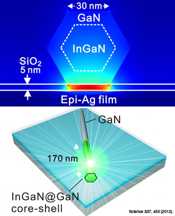
A single nanorod, placed on a thin silver film acts as a nanolaser. The resonant electromagnetic field is concentrated at the 5-nm-thick silicon dioxide gap layer sandwiched by the semiconductor nanorod and the atomically smooth silver film.
The smallest semiconductor laser emits continuously in the green, with a low threshold. The laser, based on amplification of surface plasmons, is smaller than the 3-D diffraction limit, reports Yu-Jung Lu and an international group of researchers from the National Tsing-Hua University (Taiwan), University of Texas at Austin (U.S.A.), Chinese Academy of Sciences, and National Chiao-Tung University (Taiwan) (Science; doi: 10.1126/science.1223504).
Surface plasmons are electromagnetic waves that occur at the interface between a metal and dielectric material. The laser’s plasmonic nanocavity is formed between an incredibly smooth epitaxially-deposited silver film and a single optically pumped nanorod consisting of an indium gallium nitride core, which acts as the gain medium, surrounded by a gallium nitride shell. Surface plasmons tend to lose energy quickly. In order to reduce losses, the researchers needed to create an atomically smooth silver layer. This reduces the modal volume, which reduces plasmonic losses. Graduate student Charlotte Sanders worked with co-authors Ken Shih and Jisun Kim to develop a molecular beam epitaxy process that could create a perfectly smooth surface.
Miniaturization of semiconductor lasers is key for the development of faster, smaller and lower-energy photonic technologies, including ultrafast computer chips; sensitive biosensors for detecting and treating diseases; and next-generation communication technologies. Shih says, "we believe our research could have a large impact on nanoscale technologies."