
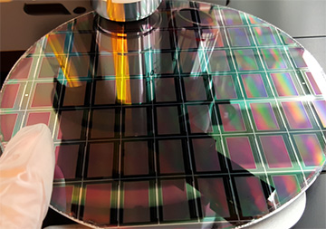
GaN-on-silicon processed microLED arrays on wafer. [Image: Wikimedia Commons/Palee93; CC BY-SA 4.0]
A recent report from the French market research firm Yole Développement has highlighted a surge in intellectual-property activity in the market for tiny microLEDs (µLEDs). According to Yole’s calculations, as of the end of last year, nearly 5,500 patents in µLED technology had been filed by more than 350 different organizations—with some 40% of the patent applications coming in 2019 alone.
Display makers, China lead the pack
As the name implies, microLEDs are microscopic light-emitting diodes that can be used as individual pixels in displays and other imaging applications. Their use has been particularly touted in high-end, high-resolution flat-panel display technologies, where they’re said to sport advantages—including a wider color gamut, greater brightness, better power efficiency and higher contrast ratios—over conventional LCD and OLED systems. But they’re also emerging as a core technology in other application areas where compactness, high resolution and luminance are important, such as VR and AR displays and so-called smart watches.
Activity by display makers has particularly driven the recent surge in patent activity, according to Yole, with the Chinese electronics company BOE Technology at the head of the list (with nearly 150 new patent families in 2019 alone), but with display firms including LG, AUO, Samsung and others also ramping up activity. Yole notes that most of these display-oriented companies “were initially dismissive of microLEDs,” but have since beefed up their efforts, driven by the potential of µLEDs as a differentiator in the high-end display marketplace.
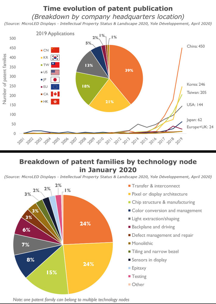
Top: According to the market research firm Yole Développement, microLED (µLED) patent activity has accelerated exponentially, with some 40% of total existing patent applications coming in 2019 alone. Bottom: Patents addressing manufacturability issues, such as mass transfer, continue to dominate IP activity in the µLED space. [Image: Yole Développement] [Enlarge image]
The Yole report also highlights the substantial advance of Chinese firms in the µLED patent game—partly a reflection, the firm notes, of the fact that China now controls almost half of worldwide display capacity. The firm views many of the Chinese µLED patents as “questionable,” but adds that some “show world-class innovation and demonstrate a strong resolve to close the gap with established rivals.”
Overcoming production bottlenecks
The technology distribution of patent activity also provides an interesting window into where this optoelectronics market is now, and where it is headed. Nearly one-quarter of the patent families tracked by Yole in this space are in “transfer and interconnect” technologies. That’s a reflection of the need to push these devices past some basic manufacturability issues to realize their market potential.
Because of the tiny size of µLEDs, a key production bottleneck for displays made with the devices is the “mass transfer” of µLED-bearing chips from the wafer (where µLEDs are grown in thin films) to the display backplane. Such transfers involve millions of µLEDs and must be executed with microscopic accuracy. As a result, conventional mass-transfer techniques are glacially slow—consuming weeks in the manufacture of a single display—and companies are on the prowl for better approaches.
Because of this, Yole notes, patents related to mass transfer continues to dominate IP activity in µLEDs. The firm highlights in particular approaches such as elastomer micro-printing and MEMS-based processes in the effort to improve production efficiency. But it also sees some interesting IP movement in niche areas related to production, such as the use of lasers for detaching µLEDs from the wafer and techniques involved optical tweezers.
Meanwhile, Yole stresses that some companies are moving past these production issues, with patents focused on efficiency and performance issues such as light extraction and shaping, display architecture and efficiency. Those activities constitute a sign, the company suggests, of increasing confidence in the industry “that mass transfer and chip efficiency conundrums could be resolved.”
More information on the Yole report can be found at https://www.i-micronews.com/products/microled-displays-intellectual-property-status-landscape-2020/.