
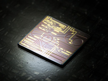
A photonic integrated circuit (PIC). [Image: Florian Lemaitre]
Entrepreneurs and others interested in technology transfer sometimes refer to the “valley of death”—the gap between innovation in the lab and commercial production. It’s a gap that’s particularly daunting for small and medium-sized enterprises (SMEs). These firms can face challenges in scaling up and demonstrating the production readiness of ideas incubated in research labs, owing to the high cost of gaining access to advanced production infrastructure and expertise.
For European photonics, one approach to bridging the valley of death has been the creation of so-called pilot lines—facilities specifically designed to give product developers, particularly SMEs, access to state-of-the art production capabilities. At least four E.U.-supported pilot-line projects have been launched since 2016, targeting areas as diverse as silicon photonics packaging, OLED manufacture, mid-IR chemical sensors and silicon nitride chips for biomedical applications.
Now, as 2018 draws to a close, two new pilot lines are joining the mix.
Ramping up in InP
The two new pilot-line entries, both managed through the Eindhoven University of Technology’s Photonic Integration Technology Center, aim squarely at benefiting the nascent market for indium phosphide (InP) photonic integrated circuits (PICs).
One of the lines, the Open-Innovation Photonics pilot for North-West Europe (OIP4NWE), is a €13.9 million project supported by the Interreg North-West Europe program, a regional cooperative encompassing eight northwest European countries under the aegis of the European Regional Development Fund (ERDF). The other InP pilot line, InPulse, will be funded through the Horizon 2020 E.U. framework program via the Photonics Public-Private Partnership (PPP), launched by the E.C. in 2013 largely through the advocacy of the Photonics21 European technology platform.
TRL: From 4 to 7
The main goal of the OIP4NWE pilot line, which launched in late November 2018, is to move the needle on the technical readiness level (TRL) of InP PIC manufacture. While PIC prototypes have moved steadily forward in the academic research lab, the organizers of OIP4NWE suggest, still-slow production processes and too-high error rates have held back the jump to commercial R&D and manufacture.
“We believe that at the moment PICs are at a technology readiness level of 4,” Victor Dolores-Calzadilla, a key figure with OIP4NWE who works in the Eindhoven electrical-engineering department, told OPN. OIP4NWE’s target, he said, is “to make it to 7.” (TRLs range from 1 for projects at the drawing-board stage to 9 for fully mature, on-the-market technologies.)
Bridging the lab and the fab
To make that jump, OIP4NWE will, over the next three years, bring academic researchers together with workers from equipment manufacturers and IC fabs, to develop equipment specifications and best-practice processes. Then, the OIP4NWE team will internally test and validate the entire production stack. The ultimate goal will be launching, by 2022, a next-gen, efficient pilot production line for InP PICs, for shared use by European SMEs.
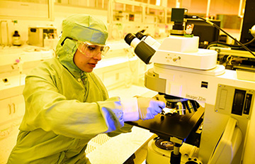
Clean room at the Eindhoven NanoLab facility, which will tackle the front-end processes of a new European pilot line for indium phosphide photonic integrated circuits. [Image: Nanolab@TU/e]
The front-end part of the process developed by OIP4NWE—production of PICs on InP wafers—will happen at Eindhoven’s existing NanoLab clean room facility. Back-end processes will take place at Vrije Universiteit Brussel, which will handle functions such as external optics for beam shaping and light coupling, and at Tyndall National Institute in Ireland, which will lead the packaging part of the effort.
In addition to these academic partners, six industrial partners will participate in OIP4NWE: AIXTRON SE (Germany); SMART Photonics, VTEC Lasers & Sensors, and Technobis Fibre Technologies (Netherlands); mBryonics Limited (Ireland); and Oxford Instruments Nanotechnology Tools (United Kingdom). The effort also includes three photonics research centers in France, Germany and the Netherlands. Some €8.3 million of the funding will come from ERDF, and the remaining €5.6 million will be kicked in by the project participants.
Open access at InPulse
The other Eindhoven-managed, InP-focused pilot-line project, InPulse, is slated for launch on 1 January 2019, according to Dolores-Calzadilla. And, he says, it’s complementary to the aims of OIP4NWE. Whereas the latter project is about “open innovation,” to improve InP PIC manufacturing and make the technology more mature, InPulse centers on open access for developers to the existing InP ecosystem. In particular, InPulse will focus on boosting the ecosystem already established by the Joint European Platform for Photonic Integration of Components and Circuits (JePPIX), a decade-old project also based in Eindhoven.
Even as it boosts access to the JePPIX ecosystem, Dolores-Calzadilla says, InPulse aims also to work toward improving the technology of InP PIC manufacture in its own sphere. But unlike OIP4NWE, which focuses on improving equipment and fabrication processes, InPulse will concentrate on developing, and then iteratively improving, the process design kits (PDKs) used to facilitate cooperation among different components of the ecosystem, including designers, software developers, fabs and prototype builders.
Other pilot lines chug ahead
Another distinction between OIP4NWE and InPulse lies in the source of the funding. OIP4NWE, as noted, is funded through a combination of contributions from ERDF and the initiative’s partners. The funding for InPulse will come through the E.U.’s Horizon 2020 program—and, specifically, through the Photonic PPP.
In that respect, InPulse will join four other PPP-supported pilot lines that were established in 2016–2017 to speed the transition from lab to market for some niche photonic technologies:
- PIXAPP is an open-access PIC assembly and packaging pilot line, focusing on silicon photonics, which is located at the Tyndall National Institute in Ireland.
- PIX4Life concentrates on scaling up silicon nitride (SiN) as a platform for visible-light detection and imaging systems for biomedical applications.
- PI-SCALE seeks to operate an open-access pilot line for organic LEDs (OLEDs) to serve customers “along the value chain.”
- MIRPHAB is building an integrated pilot line for developers of mid-IR photonic sensors for chemical sensing and spectroscopy, which it expects to have on line by 2020.
Several of these pilot lines have had news of their own of late. In mid-November, MIRPHAB announced that it is now accepting proposals from companies that want to use the pilot line to “develop and prototype new MIR devices that operate in gas-and-liquid media.”
Meanwhile, PI-SCALE—which, in mid-2018, had a share of its operation re-branded under the name Lyteus—announced, also in mid-November, the creation by two of its partner companies, Holst Centre and Fraunhofer FEP, of “the world’s longest single-device OLED.” The device is a 15-m-long OLED sheet, with an efficacy of 15 lumen/W at a light output of 1000 cd/m2, that was reportedly produced via inexpensive roll-to-roll manufacturing. The demo showed, according to Lyteus, “the possibility for continuous production of OLEDs of any length.”