
 [Nuburu]
Photonics and laser technologies are more important than ever in modern industrial manufacturing, offering highly powerful, flexible, non-contact, reliable operation. Diode lasers in particular are evolving in many critical manufacturing processes, including etching, hardening, brazing, cladding, marking and welding of metals and ceramics, and joining of components in everything from electronics to aircraft engines.
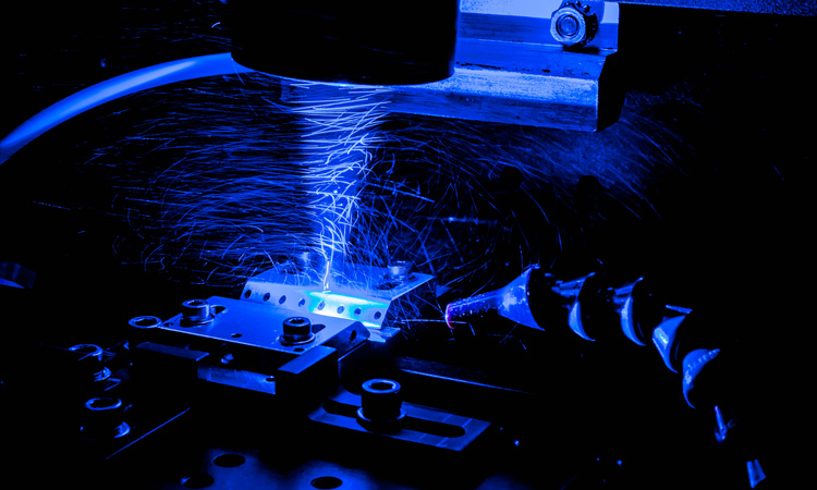
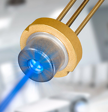
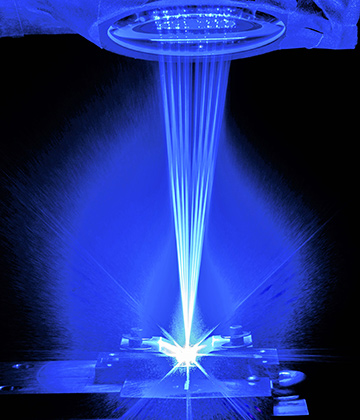 The AI 1500-W blue diode laser combines several GaAs-based laser bars to deliver 1.5 kW of power at 450 nm through 100-µm-diameter fiber focused to a spot size of 0.54 mm via a scanner, enabling defect-free welding of copper to a depth of 1.5 mm. [Nuburu]
Over the years, numerous types of lasers have found use in machining and other industrial applications. The use of lasers in industrial processing began with carbon dioxide (CO2) gas lasers in 1967. Peter Houldcroft, deputy scientific director at the Welding Institute in Cambridge, U.K., focused a 300-W CO2 laser operating in the infrared (IR) part of the spectrum at 10 µm and an oxygen assist gas to cut through a 1-mm-thick sheet of steel. To improve processing time, CO2 lasers had attained kilowatt (kW) power by the end of the decade and continued to chase power gains in the following years.
In the 1980s, fiber lasers at IR wavelengths launched in the metalworking market, disrupting the status quo. Fiber lasers, in which optical fiber is doped with rare-earth elements, achieved output powers of several kilowatts in just five years. The first 100-W fiber laser was introduced in 2000. Within ten years, fiber lasers were blazing through metal at 10-kW power levels, a feat CO2 lasers never achieved. Fiber lasers improved conversion efficiencies and reduced maintenance costs over CO2 lasers, making them a much more economical choice. Today, they have largely replaced legacy CO2 lasers in cutting and welding. But the brute force of fiber lasers can be excessive for certain delicate tasks.
The semiconductor answer
In the 1970s, the first near-IR diodes were developed for use in CD players. These were low-powered devices based on aluminum gallium arsenide (AlGaAs) semiconductor material emitting at 780 nm. Gradual advances in III-V semiconductor technology along with novel device designs began to bring diode lasers into the industrial fray.
For example, GaAs-based diode lasers are very efficient at converting electrical power to optical power in the red and IR part of the spectrum, and are used today for optical pumping and as direct sources in metal cutting. Semiconductors introduced scalability at mass volumes, and as power-conversion efficiency saves operating costs, the technology grew, particularly in communications, which helped set the stage for its growth in other applications.
In 2007, researchers at Jenoptik in Jena, Germany, demonstrated the first kW-class IR laser bars measuring 1 cm. In the next decade, researchers at Ferdinand-Braun Institute in Berlin improved operating conversion efficiency from 35% to more than 65% for devices operating at 980 nm. But for kilowatt-class industrial processes like cutting, welding and soldering, IR has drawbacks. For applications using copper and gold, the metal absorbs only about 5% of the powerful incident thermal energy of IR lasers, causing wasteful spattering, jagged edges and defects that can weaken a weld.
Green and blue wavelengths are far more readily absorbed by many metals than IR, making the weld smoother and more easily controlled. In fact, copper absorbs blue light 13 times more than it does IR wavelengths; gold absorbs 66 times more blue than IR. Fabricators using these metals have long been eager for laser tools at alternative wavelengths that offer dollar-per-watt efficiencies.
Progress in ramping up blue diode power and efficiency has happened faster than for IR diodes, as the semiconductor processes established for IR paved the way for blue sources.
Gallium nitride (GaN) semiconductor material is particularly useful for emitting in the UV, blue and green regions of the spectrum, but it presents challenges in terms of its hole mobilities, temperature sensitivities and high band gap of 3.42 V. In the late 1990s, Isamu Akasaki and Hiroshi Amano at the University of Nagoya and Shuji Nakamura at Nichia Chemicals, Japan, invented the first practical blue LED, which appeared in Blu-ray DVD players in 2006—24 years after the CD player.
According to Jean-Michele Pelaprat—chief marketing and sales officer and cofounder of early-stage blue diode company Nuburu in Centennial, CO, USA—blue-emitting GaN semiconductors are still about a decade behind red-emitting GaAs in technological maturity. But the GaN efficiency and lifetime have made huge progress.
“Only in the past five years has GaN semiconductor technology matured enough to enable higher-power blue diodes for industrial applications,” said Pelaprat.
While it took a long time for science to master the first blue diodes, the progress in ramping up power and efficiency has happened faster than that of IR diodes, since the semiconductor processes established for IR had already paved the way for blue sources.
Thomas Brandes, senior product manager at optoelectronics manufacturer Osram Opto Semiconductors (Regensburg, Germany), says, “It’s been really amazing to see the technology improve from the first commercial direct green diode in 2012 to kilowatt packages in the blue today. The development of high-powered blue diodes has happened quickly in just a few years.”
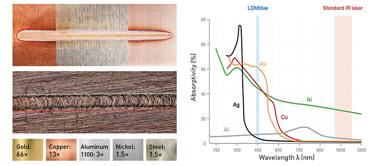 Left: A blue laser leaves smooth marks in copper (top) and gold (center). The blue-to-IR absorption ratio of commonly welded metals (bottom). [Laserline GmbH, Germany / Nuburu]
Right: Compared with absorptivity in the IR region of the spectrum, the absorptivity of commonly welded materials like gold (Au), copper (Cu) and nickel (Ni) is much higher at 450 nm, where high-powered blue diode lasers shine with >1 kW of output power. Higher absorption rates mean blue lasers achieve similar processing results using less optical power. [Laserline, NASA]
The push for brighter blue
Single-mode blue diodes used in low-power Blu-ray DVD players and lighting applications today have optical output powers ranging from tens of milliwatts to a few watts. Currently, multimode blue diodes can reach increased output powers of up to around 5 W. These can be doubled up to reach, for example, 20 W for 3D printing or engraving metal—achieving what a CO2 laser can using a fraction of the electrical power. But achieving the kilowatt output powers necessary for industrial metalworking in short wavelengths would take a coordinated effort across multiple government, academia and industry collaborations.
Achieving the output powers necessary for industrial metalworking in short wavelengths would take a coordinated effort across government, academia and industry collaborations.
In 2016, Osram began a three-year R&D effort to push advances in industrial diode lasers across the spectrum. The research project, called “BlauLas,” from the German term for blue laser, joined Osram with the Max Born Institute for Nonlinear Optics and Short Pulse Spectroscopy (Berlin, Germany), and industrial laser companies Laserline (Mülheim-Kärlich, Germany) and Coherent DILAS (Mainz, Germany). The goal of the BlauLas project, funded by the German government, was to develop a new approach to kilowatt-power direct blue lasers.
BlauLas project coordinator Harald König at Osram and his team focused on fabricating high-quality, homogenous epiwafers, or ridge waveguide laser bars, each with numerous 450-nm single emitters isolated via etched grooves. When driven with 60 A, the first result was 98 W of max output power from a single 1-cm-wide laser bar with 23 emitters, well above their target of 50 W. The scalable design reached 700 W of power coupled via 600-µm fiber in early 2018, with estimated lifetimes beyond 5000 hours.
“Over the last decade we improved the peak efficiency of blue GaN laser diodes from 15% to beyond 45%,” said König, “and in parallel increased the output power.”
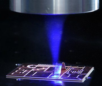
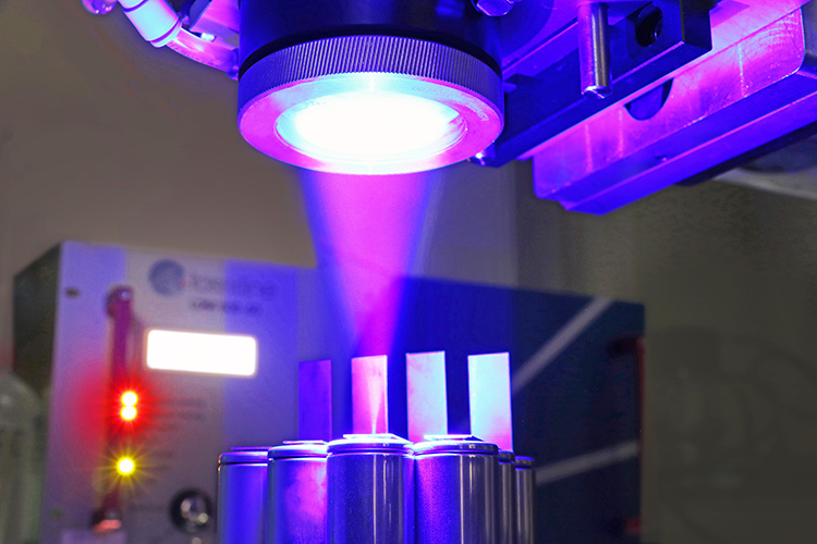 The LDMblue 1000-40 high-powered diode offers 1000 W of CW power at 450 nm, opening up applications in spatter-free processing of copper and other metals, such as in welding battery interconnections (left) and copper wire terminals. [Courtesy of S. Britten, Laserline]
Kilowatt-class systems
At Photonics West in 2019, Laserline presented results on fiber-coupling of two stacks of GaN blue diode bars, reaching 1000 W of power at 450 nm with 25% electro-optical efficiency. BlauLas had increased the output power of a blue direct diode laser by an order of magnitude. Shortly thereafter, Osram launched a commercial laser bar chip with 50 W of 445-nm optical power, 7.5% fill factor and a 38% conversion efficiency.
What is BPP?
The brightness of a laser is called the beam parameter product or BPP, a standard comparative metric of beam quality. Blue high-powered laser diode modules have reached kilowatt output power with superior conversion efficiency compared with green or IR lasers, but their beam quality is lower.
The BPP is the product of a laser’s smallest beam radius and its divergence. This is useful for understanding beam quality, and smaller is typically more desirable. The smaller the BPP, the smaller the spot size a laser can achieve, and thus a smaller diameter fiber can be coupled to the laser to focus more intensely on a single spot for better precision welding.
The typical BPP of a single-mode near-IR laser around 1 µm would be approximately 0.3 mm-mrad. The BPP of high-power blue diodes are quite limited in comparison, ranging from 11 mm-mrad for single- emitter CW diodes, to 60 mm-mrad for CW laser diode bars at 450 nm.

Commercially available high-powered blue diode laser sources with 450-nm wavelength.
As the output power increases, high thermal conductivity of the GaN substrate causes thermal crosstalk between neighboring emitters, which can cause damage to the bar. Solutions include mounting each bar on microchannel heat sinks and using a fast-axis collimation lens to collimate the optics. Subsequent studies presented in 2020 concluded that an optimal lateral fill factor of 7.5% with 30 µm emitter widths and 400 µm pitch per bar would enable 1.6 kW of output power with conversion efficiencies up to 40% for a fiber coupled system.
Laserline’s LDMblue series of industrial solutions for copper processing uses Osram’s bar emitters coupled into fiber to achieve kW-class systems operating at 445 nm. The 1 kW LDMblue 1000-40 system, launched in February 2019 for welding of very fine copper sheets up to 0.5 mm thick, claims a beam parameter product (BPP) of 40 mm-mrad. The 1500-W system followed in June 2019.
In April 2020, Laserline announced the availability of 2-kW systems with 60 mm-mrad beam quality for testing in laboratories, which promises to improve welding time and penetration depths up to 1 mm. The modular systems fit in a 19-inch rack for ease of integration with existing systems. The company claims that the diode creates welds precise enough to handle thin copper sheets in smartphone batteries, and that it even works for underwater welding, opening up new applications in ship and bridge repair.
Keeping it cool
As output power increases to the kW scale necessary in industrial processing, so does the heat. Whether in a TO can, bar, or stack of emitters, the cooling requirements on diode systems are challenging. Cooling can be passive, relying on natural cooling, which is the case with Osram’s blue single-emitter TO can. Or cooling can be active via circulating air, water or refrigerant. Conductive cooling incorporates a metal heat sink with fins and baffles, which is commonly combined with a fan.
 Single-emitter blue diode, packaged in a standard TO can. [Courtesy of Osram]
The first high-power diode laser bars used microchannels carved into them to dissipate the heat generated from their IR emission. This technique makes the bars vulnerable to corrosion that could affect diode reliability and performance. Microchannel cooling also takes up some space on the bars, reducing the fill factor. Osram found that a more reliable way to diffuse heat is to mount the bars on an actively cooled heat sink. Future designs may focus on reducing thermal crosstalk to help reduce heat.
“If you increase the power in diode lasers, careful homogenous management of the increased heat is important. The cooling method depends on the application and should be reviewed accordingly,” said Brandes. “In the end, blue diode technology is very reliable and efficient in the long term. We’ll continue to find ways to optimize and make a good product even better.”
Modular solutions
Launched in April 2015, Nuburu, which translates to “new blue” in Japanese, took a different approach. The company mounts Osram’s GaN single-emitter diodes on a chip in series, which reduces operating current and enables responsive control of power and pulse modes. Combining multiple single emitters, each in rugged compact packaging, takes advantage of established, robust and high-yield semiconductor fabrication technology. Even more importantly, combined single emitters can achieve higher brightness than diode bars, which is important for welding applications.
The modular architecture hinges on the placement of a small micro-lens on each emitter, individually aligned to collimate the output. Several tens of low-power emitters can combine to create a 50-W source, which can then be scaled up to 1.5-kW lasers and up using spatial and polarization combiners to focus the combined beams into a fiber. The devices use microchannel water cooling.
Nuburu introduced its first high-powered blue diode in 2017, the AO-150 (pronounced “ah-oh,” which means blue in Japanese) with 150 W of continuous wave (CW) power and a BPP of less than 15 mm-mrad. Within a year, the company had a 500-W unit with a BPP of 30 mm-mrad, which improved into a 600-W product. The AI 1500 (“ah-ee” in Japanese for deep blue) followed earlier this year, delivering 1.5 kW with a BPP under 11 mm-mrad from a 100 µm 0.22 NA aperture fiber. The brightness of the AI-1500 enables the use of a scanner that is ideal for delivering fast and defect-free copper welding at 450 nm.
Tests show that a lifetime of more than 25,000 hours at 200 W and 650 W should be sustainable for the AO-200 and the AO-650. Testing has proven that the kW-class brightness of the AO and AI series can effectively weld copper and aluminum sheets ranging in thickness from 0.007 mm to 2.5 mm. Another application these lasers can address is the welding of hairpin terminals in electric motors, the density of which can be increased in the motor with no spatter or porosity in the weld.
E-mobility
Transportation is undergoing a massive shift not seen since Ford rolled out the Model-T. Rather than affordability, however, the sector is focused on accountability as it develops green, regenerative, all-electric vehicles. The electrification of vehicles or so-called “e-mobility” technology, which encompasses the use of electric powertrain, information and communications in-vehicle and inter-fleet, helps reduce harmful emissions and shift the reliance on petroleum to greener sources.
This growing new field is driving the need for better fabrication processes for electric motors and batteries. Electric-vehicle batteries require processing of more copper, nickel and lithium than traditional combustion motors, which include more cast iron, steel and aluminum.
Reliability and power-conversion efficiency are paramount in electric-vehicle batteries, which can be improved with blue diode wavelengths to achieve stronger, defect-free welds.
Laser processing is used in e-mobility for cutting materials, manufacturing cell compartments and welding conductor materials to battery cells. While near-IR fiber sources are popular for welding these materials quickly and efficiently, the copper materials in these applications are often only hundreds of microns in size and are damaged by IR sources.
Nuburu’s Pelaprat explains, “Many battery and e-mobility applications have equipment with very thin copper foils of less than 2.5 mm thick. Red and IR wavelengths reflect off the metal; they require so much energy to start the welding that the material is vaporized, leading to spatter and defects. With blue light, the vaporization phase is rarely reached, leading to a spatter-free and defect-free process.” Reliability and power-conversion efficiency are paramount in electric-vehicle batteries, which can be improved with blue diode wavelengths to achieve stronger, defect-free welds.
 A blue laser welds copper ribbons to a direct copper bonded substrate, a common ceramic substrate based on Al2O3 coated with copper.[RWTH Aachen University/Fraunhofer ILT]
In 2019, researchers at Rheinisch-Westfälische Technische Hochschule (RWTH) Aachen University and Fraunhofer Institute for Laser Technology in Germany conducted quantitative studies of Nuburu’s AO-150 blue laser diode and its performance in micro-welding of copper foils only 125 µm thick. Laser researcher Marc Hummel at RWTH Aachen University and colleagues found that the improved absorption of 450-nm light allows heat conduction welding with no significant pore formation in the weld seam, at welding depths between 100 µm to 648 µm for two types of copper alloy.
As the process involves heating the metal until it temporarily reaches a flowing molten phase, a special kind of process is required to shape these small components before they solidify. To address this unique process, The German Research Foundation funded The Collaborative Research Center at RWTH Aachen in 2014, focused on new scientific approaches and technologies for precision-melt-based engineering processes.
Multi-kilowatt blue diodes also show promise in applications beyond e-mobility. Long resonator lengths and microchannel cooling of GaN laser diodes creates thermal rollover that offers the possibility of tuning them to different emission wavelengths for use in wavelength division multiplexing—a technique for sending multiple signals down a single optical fiber in communications. High-power blues also have immediate potential for melting copper powder in 3D additive printing and laser metal deposition.
“High-power blue lasers for material processing are ready now,” said Brandes. “And they will open the door for more research and many new applications in the years to come.”
Valerie C. Coffey is a freelance science and technology writer and editor based in Palm Springs, CA.
References and Resources
-
K. Price et al. “KW-class industrial diode lasers comprised of single emitters,” Proc. SPIE 7583, 75830E (2010).
-
A. Balck et al. “700 W blue fiber-coupled diode-laser emitting at 450 nm,” Proc SPIE 10514, 1051403 (2018).
-
M. Baumann et al. “1000 W blue fiber-coupled diode-laser emitting at 450 nm,” Proc. SPIE 10900, 1090005 (2019).
-
J.P. Feve et al. “Scalable blue laser system architecture,” Proc. SPIE 11262, 112620P (2020).
-
M. Hummel et al. “New approaches on laser micro welding of copper by using a laser beam source with a wavelength of 450 nm,” Journal of Adv. Joining Process. 1, 100012 (2020).
-
M. Behringer and H. König, “Blue high–power laser diodes—Beam sources for novel applications,” PhotonicsViews 17, 2 (2020).
-
H. König et al. “Blue high power InGaN semiconductor laser diodes,” Proc. SPIE 11262, 112620Q (2020).
Editor's note: A correction has been posted for this article