
 [Courtesy of the authors]
In 1931, future Nobel laureate Maria Göppert-Mayer published her Ph.D. thesis on the theory of two-photon absorption in atoms. Not until 30 years later was the phenomenon observed experimentally, and it took another three decades for it to find application in the life sciences through two-photon-induced fluorescence microscopy.
Meanwhile, in 1997, Shoji Maruo and coworkers at Osaka University, Japan, pioneered another use of two-photon absorption: 3-D microfabrication via the solidification of photopolymers. This technology today is often called two-photon 3-D laser nanoprinting, in analogy with the megatrend of 3-D printing, or macroscale additive manufacturing. But as the name implies, 3-D nanoprinting takes things to a much finer scale. In this feature, we look at where the technology stands, and where it’s going.
Two-photon magic
What is the “magic” of two-photon absorption, as opposed to one-photon absorption? The answer lies in the tails of a tight laser focus.
In 3-D printing involving lasers and a typical liquid photoresist, light induces a chemical reaction in the photoresist, mediated by a molecule known as a photoinitiator that is mixed into the resist at concentrations of around 1%. The reaction brings the liquid resist, which often begins as a monomer, into a cross-linked solid state—a polymer. After scanning the laser focus in three dimensions to write the desired architecture with a “pen of light,” the remaining liquid is washed out using a solvent such as acetone in the so-called development phase.
The “magic” of two-photon absorption, as opposed to one-photon absorption, lies in the tails of a tight laser focus.
The amount of local cross-linking depends on the accumulated absorbed dose. Thus, for one-photon absorption, the tails of the laser focus can add up over multiple exposures, strongly distorting the desired pattern—a tail with a 1% intensity relative to the focus maximum, for example, will add up to 100% of that maximum when summed over 100 exposures. In sharp contrast, for two-photon absorption, the absorbed dose is proportional to the square of the local intensity. Therefore, a 1% tail contribution will have a strength of (0.01)2 = 0.0001 relative to the focus maximum. Summing that over the same 100 exposures now leads to an effective exposure for the tail area of a negligible 1%.
Clearly, two-photon absorption isn’t necessary for applications like planar 2-D optical lithography, nor even for 3-D lithography of geometrically simple objects such as individual dots or lines. It becomes crucial, though, for complex 3-D architectures requiring many different individual exposures—and enables the building of objects with incredibly fine-scale features.
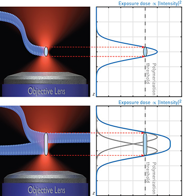 Voxel size and Sparrow criterion: In two-photon laser nanoprinting, light (red), tightly focused through an objective lens and scanned through an initially liquid photoresist, creates a polymerized path (blue). Given a sharp polymerization threshold, voxel size can be much smaller than the wavelength (top). But if individual doses for two adjacent voxels (gray curves) add up in the photoresist (bottom), the voxels merge, limiting resolution under the Sparrow criterion. [Courtesy of the authors]
Beyond the wavelength of light
In 3-D laser nanoprinting, an individual point exposure leads to a so-called voxel, the 3-D volume element named in analogy to the 2-D picture element, or pixel. The voxel size can be much smaller than the wavelength of light because the photoresist effectively acts as a strong nonlinearity: In the so-called threshold model, below a certain minimum exposure dose, the material is not sufficiently cross-linked, and the developer washes it out, while above this threshold dose the material remains.
In this model, arbitrarily small voxels or line widths could be obtained—there is no diffraction limit for the obtainable minimum feature size. When writing two adjacent exposures, however, the doses add up, and below a certain minimum distance between the exposures, the two-dose maxima merge into one, and a larger, single voxel results. This transition, called the two-photon Sparrow criterion, means that for a lens with numerical aperture (NA) of 1.4, the minimum lateral separation is about one quarter of the free-space wavelength, λ/4—for example, the separation between voxels must be 200 nm for λ = 800 nm.
The axial resolution is not quite so fine. When using a single objective lens, light is focused from only one half-space; hence half of the wave vectors of light are missing, and the voxel is elongated in the axial direction by at least a factor of two. Typical best values are actually around 2.5, leading to an axial resolution around 500 nm. Stimulated-emission-depletion (STED) tricks can further improve this value.
 Additive manufacturing: Speed versus feature size
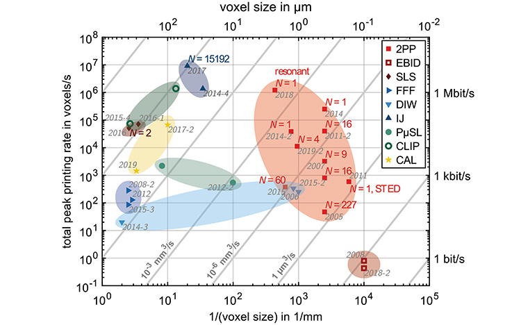
Additive-manufacturing technologies compared by inverse voxel size versus printing rate; parallel gray diagonals are lines of constant 3-D-printed volume per second. Additional details and references are at www.osa-opn.org/link/3-D-nanoprinting. [V. Hahn et al., unpublished]
Getting to two-photon absorption
The use of femtosecond lasers is central to making two-photon absorption sufficiently probable for 3-D nanoprinting. These lasers bring an amazing concentration of photons in space and time—for example, an average laser power of a mere 10 mW, delivered in 100-fs pulses at a repetition rate of 100 MHz and focused to a typical effective laser spot area of 10−9 cm2, leads to a peak light intensity of about 1012 W cm−2. That corresponds to the power of a thousand 1-GW nuclear power plants, concentrated to an area the size of your thumbnail.
The equivalent photon flux density from such concentration is about 1031 photons s−1 cm−2. Multiplying that number by a typical molecule’s two-photon absorption cross section, 10−50 cm4 s photons−1 (a value that defines the unit 1 GM, named in honor of Maria Göppert-Mayer), we obtain an effective area or cross section of 10−19 cm2. That area, while small compared with the typical one-photon-absorption cross section of molecules in solution at room temperature, is large enough for useful two-photon printing.
Evaluating printing speed
Two-photon 3-D laser nanoprinting, as described above, is a serial writing process—but that does not necessarily make it a slow one. One metric for speed comparisons among different additive-manufacturing approaches is the rate in voxels per second—which can be understood as the speed at which digital information (for example, from a digital blueprint) is converted into hardware.
The chart below plots several printing technologies’ level of “fineness” (measured by inverse voxel size) against their writing speed in voxels per second, across eight orders of magnitude. The straight diagonals draw lines of constant printed volume per time. A look along those diagonals shows that, although two-photon printing appears slow in absolute volume printing rate, it is far from slow in the voxel printing rate, in view of the very fine voxel sizes it resolves. The absolute volume rate alone is not meaningful; if it were, one could attain a new world speed record by exposing a bucket full of photoresist to the flash of a pocket lamp!
It is also interesting that—counterintuitively—the total printing speed of two-photon setups with multiple laser foci has been slower (so far) than the best single-focus printing. This, again, largely results from the physics of two-photon absorption. In a single-focus setup—assuming that one is not technically limited by the speed of scanning the laser focus, but only by laser power—it follows that, when the focus speed is increased by a factor of ten, the two-photon absorption rate must be increased by the same factor to keep exposure conditions constant. Because two-photon absorption depends quadratically on laser intensity, however, the laser power need to be increased by only a factor of 10½, or around 3.16. In contrast, a factor-of-10 increase in printing speed by using 10 laser foci rather than a fast-scanning laser focus requires a tenfold increase in total laser power.
The situation changes when increasing the focus speed is no longer possible. Today, focus speeds on the order of 0.1 m/s are state of the art, and resonant galvo-scanners support speeds as large as a few meters per second. To write complex 3-D architectures, however, the acceleration timespans of the galvo-scanners for foci inside and outside of the microscope objective’s field of view (typically some 300 µm in diameter) become more and more problematic, resulting in hard-to-correct artifacts of the actual focus motion. Getting the data from the control computer to the galvo-scanners synchronized with the light modulator also becomes increasingly difficult, boosting overhead times.
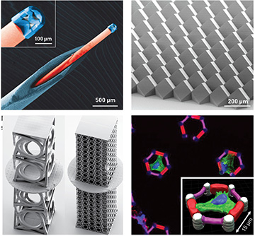 Gallery of two-photon-printed architectures: (Clockwise from top left) Micro-optical triplet lens for endoscopic applications in medicine; Wafer-scale micro-optical components; Scaffolds for biological cell culture with cells within; Chiral mechanical metamaterial enabling twist degrees of freedom. [T. Gissibl et al., Nature Photon. 10, 554 (2016); courtesy of the authors; reconstructed from laser scanning confocal fluorescence microscopy / courtesy of the authors, following B. Richter et al., Adv. Mater. 29, 1604342 (2017); T. Frenzel et al., Science 358, 1072 (2017)]
As these considerations suggest, comparing printing speeds of different technologies, and even different two-photon-printing setups, holds many complications, and such comparisons often must be taken with a grain of salt. Although ideally one should compare the same 3-D benchmark structures for all technologies, in practice the field has not yet reached this level of consistency and maturity.
Three challenges: Finer, faster, more
Even as the technology is still maturing, state-of-the-art two-photon printing with commercially available infrastructure has allowed the construction of some dazzling microscale architectures (see some examples at left). The technology’s commercialization started more than a decade ago, in 2007, and has increased tremendously in the last few years. So far, the market has largely been in academia, with users from optics and photonics, mechanical engineering, chemistry, biology and medical faculties.
However, recent work has established that two-photon printing allows for the making of wafer-scale masters for so-called 2.5-D, complex micro-optics in industry—including freeform surfaces. Once the otherwise difficult-to-obtain master has been two-photon-printed, it can be used for replication by soft-imprinting, hot embossing and other mass-fabrication-compatible industrial approaches.
Looking ahead, like 3-D printing generally, 3-D laser nanoprinting confronts three development challenges: making ever finer structures, faster, and in more different materials. Of these three, the “more materials” challenge is perhaps the most urgent. The vast majority of published applications thus far have involved only a single material, with a single fixed set of material properties; in addition, most structures presented have been passive ones, and cannot be cleaved or degraded using mild processes. In recent years, researchers have pursued three different approaches to address the “more” challenge.
Multiple resist cartridges
This approach takes its cue from today’s 2-D graphical inkjet printers. After writing part of a 3-D micro-architecture into a first photoresist, the structure must be developed and cleaned, after which a second resist can be infiltrated, written into and developed. In previous years, these steps were performed manually: the operator had to go back and forth between the two-photon printer and the chemistry lab multiple times, with tedious re-alignments with sub-µm precision in all three dimensions.
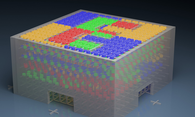
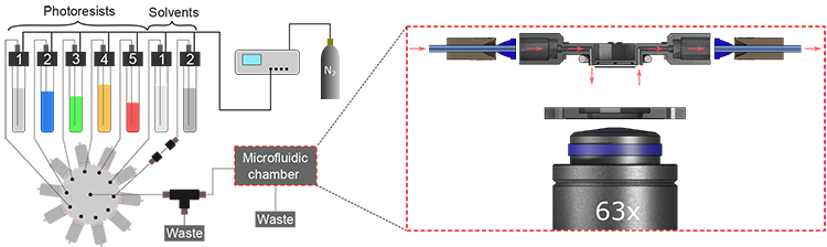 Microfluidics meets two-photon nanoprinting: Integrating a microfluidic chamber (not to scale) into a commercial two-photon printer allows the creation of 3-D architectures composed of many dissimilar materials (see, for example, blueprint shown in the opening spread). [F. Mayer et al., Science Adv. 5, eaau9160 (2019); published under a Creative Commons license (CC-BY 4.0)]
The use of a dedicated microfluidic chamber integrated into the two-photon printer, connected to a delivery system of all involved photoresists and developers, has recently made this task much simpler. The system imposes some challenges: its high-end optics can limit the free working distance to a few 100 µm, which in turn limits the height of the microfluidic chamber. Meanwhile, a thin aberration-corrected glass substrate, only 170 μm thick, limits the excess pressures one can apply to about 3 bar—even as the variety of materials involved, ranging from photoresists as viscous as honey to some solvents that are less viscous than water, implies a huge variation of pressures needed to push the liquids through the narrow, microfluidic channels.
Nevertheless, such a microfluidic system, compatible with a state-of-the-art commercial two-photon printer, has successfully been designed, built, and used to create, in a first proof-of-concept, a 3-D deterministic fluorescent security feature, created out of seven different liquids: four different photoresists doped with different semiconductor CdSSe core-shell quantum dots or dye molecules; one non-fluorescent resist serving as 3-D scaffold; and two different solvents.
Multiple material properties from a single resist
A second possibility—which is complementary to and can be combined with the multiple-resists approach described above—is to use only a single photoresist throughout the entire 3-D printing process, but change a suitable stimulus during the writing, controlled for each voxel. In response to this stimulus, the resist properties change, leading to the possibility of many different material properties from a single resist.
Conceivable stimuli that might be adjusted include laser power, laser wavelength or polarization, the strength and direction of a quasi-static electric field or magnetic field, or some other parameter. In a 2019 demonstration, varying the laser power allowed changes in the degree of cross-linking of a hydrogel combined with a bisacrylamite cross-linker, leading to a controlled variation of the resulting material’s Young’s modulus and a factor-of-ten variation in its thermal-expansion coefficient. This, in turn, enabled the creation of bi-material structures that could be activated to large motions either by temperature changes of just a few degrees Celsius or by focused light only a few mW in power.
“Meta-ink”
Yet another approach enabling many different effective material properties in a single workpiece is the “meta-ink” approach—an analogue of dithering in 2-D graphical printing, based on recent advances in 3-D metamaterials. Metamaterials are engineered, micro- or nanostructured materials that can produce a wide variety of different mechanical, electrical and optical properties. These properties derive not only from chemistry, but also from structure.
For two-photon printing, creating this metamaterial substructure in 3-D printed materials poses large demands on the number of voxels that need to be printed. In recent metamaterials, up to a thousand metamaterial crystal unit cells have been realized, overall comprising between one and ten billion voxels in 3-D. Clearly, for real applications, orders of magnitude more metamaterial unit cells are required, and the voxel and unit-cell size needs to be shrunk.
This brings us back to the two other challenges for future development: “finer” and “faster.” On the finer-features side, STED-inspired approaches have led to smaller features in 3-D—conceptually without any diffraction barrier. Although the optical potential for features on the scale of tens of nanometers is there, progress toward that goal has stagnated in recent years, and help will be needed from chemistry to get there.
How fast can two-photon printing go?
Regarding the “faster” challenge, we expect substantial progress in the next several years. Even with current technologies, the speed of single-focus two-photon printing can be boosted by an order of magnitude or perhaps more by pushing on several technical levers.
One such approach is increasing the focus speed—though here, a natural limit does exist. As the focus speed increases, eventually it reaches a point at which the focus moves by an appreciable fraction of the voxel size during the interval between adjacent femtosecond optical pulses. For example, at a focus speed of 10 m/s and a pulse repetition rate of 100 MHz (10 ns between pulses), subsequently exposed voxels are already separated by as much as 100 nm. If this separation exceeds the voxel size, adjacent voxels are no longer connected and a smooth piece cannot be created. Increases in focus speed also require corresponding decreases in focus-positioning error, along all three spatial dimensions, to ensure that structural quality does not deteriorate.
Another way to boost total printing speed is to use multiple different laser foci, scanned in parallel or even independently. In principle this increases speed by a factor equal to the number of laser foci—although here again there are limits. When the different foci come too close to each other, for example, their fields can interfere, which could lead to a loss of axial resolution in 3-D. At the other extreme, the maximum foci separation is limited by the finite field of view of the microscope lens.
Furthermore, available laser power becomes an issue at some point. Our lab uses femtosecond laser oscillators with an average optical power of 3 W; powers much larger than that cannot be sent through high-numerical-aperture microscope objective lenses without risking damage. Perhaps chemistry will come to the rescue by providing more sensitive resists.
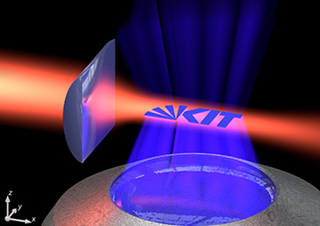 In light-sheet nanoprinting, light of two wavelengths is delivered: One in a light sheet that defines the z plane, and one in a second beam from below that defines the x-y pattern. The “AND-photoresist” is chemically developed to polymerize only if light of both wavelengths is present. [V. Hahn et al., unpublished]
A light-sheet approach
Combining the improvements mentioned above, printing rates in the range of 107 to 108 voxels/s will likely become possible. Getting beyond that to more dramatic print-speed improvements, however, will require radically new approaches.
One approach, currently under development in our lab, has been inspired by the rise of light-sheet optical microscopy. Here, a first laser focus through a cylindrical lens defines a thin sheet of light parallel to the x-y plane at wavelength λ1. A second laser, at a different wavelength λ2, projects an entire 2-D image into the plane defined by the light sheet, via a second microscope lens along the optical axis z. This 2-D image, created using a spatial light modulator, can easily be composed of a million pixels.
A key element of this approach is the requirement of an “AND-photoresist” that will polymerize only if light of both wavelengths λ1 and λ2 is present in a certain volume element. Two-photon absorption, in the nonlinear-optics sense, is not needed; rather, the light-sheet 3-D-printing approach uses two successive one-photon absorption processes, which can be induced by two different continuous-wave lasers or two different light-emitting diodes rather than by a single femtosecond laser. Nevertheless, the overall process is effectively nonlinear. The thickness of the light sheet determines the resolution in the z direction.
In preliminary tests of a prototype resist of this logical “AND” type, we have found that, if the initiator molecule’s intermediate-state lifetime is chosen suitably, such resists can be orders of magnitude more photosensitive than current, two-photon-absorption-based resists, enabling substantial increases in speed. We believe that the light-sheet approach, if successfully scaled up, could catapult 3-D printing at the microscale to a new level. Conceivably, 3-D-printing processes that take 24 hours today might take tens of seconds, thanks to the tricks possible by combining advanced optics and novel photochemistry.
From the lab to the home?
Considered a scientific curiosity when it emerged two decades ago, two-photon 3-D laser nanoprinting has since come a long way. Even when the technology was first commercialized around 12 years ago, some still argued that “nobody needs 3-D.” Today, more than a thousand users worldwide enjoy the versatility and reliability of 3-D additive-manufacturing technology for the making of microscale objects that seemed difficult if not impossible to make previously.
It’s even possible that, with future advances, the technology might go beyond academic and industry users—even arriving in people’s homes as a sort of “personal fabricator.” Before we assume that no one would be interested in such a thing, we would do well to recall that, in 1977, Ken Olsen, the founder of Digital Equipment Corporation, famously argued that there “is no reason anybody would want a computer at their home.” Four decades later, the number of personal computers and mobile phones is comparable to the overall population in many countries. With that example in mind, we are convinced that the most interesting times for 3-D laser nanoprinting lie ahead.
We acknowledge support by the Deutsche Forschungsgemeinschaft (DFG) under Germany’s Excellence Strategy and by the Carl-Zeiss-Foundation through the Excellence Cluster “3D Matter Made to Order” (3DMM2O , EXC-2082 – 390761711) and the associated HEiKA Graduate School “Functional Materials,” by the Karlsruhe School of Optics & Photonics (KSOP), by the Max Planck School of Photonics (MPSP), by the Helmholtz program Science and Technology of Nanosystems (STN) and the associated Virtual Materials project (VIRTMAT), and by the Nanostructure Service Laboratory (NSL) of KIT.
Vincent Hahn, Frederik Mayer and OSA Fellow Martin Wegener are with the Institute of Applied Physics and the Institute of Nanotechnology, Karlsruhe Institute of Technology, Karlsruhe, Germany. Michael Thiel is Chief Science Officer of Nanoscribe, Eggenstein-Leopoldshafen, Germany.
References and Resources
-
M. Göppert-Mayer. Ann. Phys. 401, 273 (1931).
-
W. Kaiser and C.G.B. Garrett. Phys. Rev. Lett. 7, 229 (1961).
-
W. Denk et al. Science 248, 73 (1990).
-
E. Wu et al. Proc. SPIE 1674, 776 (1992).
-
S. Maruo et al. Opt. Lett. 22, 132 (1997).
-
E. Rittweger et al. Nat. Photon. 3, 144 (2009).
-
J. Fischer and M. Wegener. Laser Photon. Rev. 7, 22 (2013).
-
C. Barner-Kowollik et al. Angew. Chem. Intl. Ed. 56, 15828 (2017).
-
M. Hippler et al. Nat. Commun. 10, 232 (2019).
-
F. Mayer et al. Sci. Adv. 5, eaau9160 (2019).
-
M. Kadic et al. Nat. Rev. Phys. 1, 198 (2019).
For additional references and resources, see www.osa-opn.org/link/3-D-nanoprinting.