
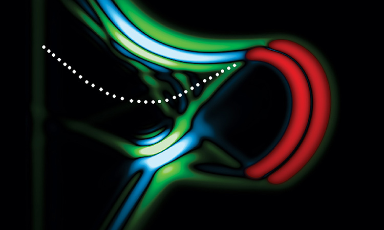
 A metasurface bends visible light inside a lithium tantalite crystal to produce “synchrotron” radiation (blue and green) via an accelerating light pulse (red), on a scale a thousand times smaller than massive synchrotron facilities around the world. [Image by Meredith Henstridge, University of Michigan, for M. Henstridge et al., Science 362, 439 (2018)]
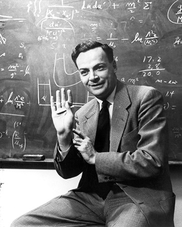 Richard Feynman at Caltech. [Caltech Archives / Photograph used with the permission of Melanie Jackson Agency, LLC]
For centuries, grand predictions were the realm of soothsayers and self-proclaimed prophets. In the age of science, studies of the future tend to be extrapolations from current trends.
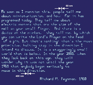
But Richard P. Feynman’s classic talk, “There’s Plenty of Room at the Bottom,” remains a stellar example of physics prognostications that not only came mostly true, but in some cases exceeded expectations. On 29 December 1959, speaking at an American Physical Society (APS) meeting, he took his audience on a wandering, speculative tour of tiny technology and problems that might have seemed insurmountable near the end of the vacuum-tube era.
Some of Feynman’s conjectures about the “staggeringly small world” seemed like a cross between 19th-century carnival hoaxes and science fiction. Could humans copy an encyclopedia onto the head of a pin? Could they build tiny motors by rearranging atoms? Could molecular machines build copies of themselves? Could a cube the size of a dust mote hold the contents of all the world’s libraries? Could an array of infinitesimal antennas send out a directional beam of high-intensity of light? He peppered his talk with insistent comments and questions: How would we read it? I don’t know why this hasn’t been done yet! What good would it be to see individual atoms distinctly?
At the time of his idiosyncratic speculations, Feynman, the highest-paid professor at the California Institute of Technology (Caltech), USA, had gained recognition in the physics community for his work in quantum theory and superfluidity, but, six years before his Nobel Prize, he was not yet famous among the general public.
Feynman spoke at a time when no artificial source of coherent light existed, computers filled entire rooms and the integrated circuit was in search of a patent. The noted physicist might not have used the precise terminology—or, for that matter, the measuring units—scientists employ today. He didn’t mention photonics, or plasmonics, or even the laser, which would only be invented in the following year.
Feynman’s conjectures presaged some of the hottest areas of present-day research in optics and nanotechnology, from imaging to circuitry to robotics.
The future Nobel laureate “focused on electrons and he focused on atoms, but he didn’t focus on photons,” says OSA Fellow Teri Odom, professor of chemistry and materials science at Northwestern University, USA. Upon reading the text of the six-decades-old speech, she was struck by how the Caltech physicist approached tiny machines as if they were classical-scale objects, without accounting for device architectures that accommodate coherence and quantum behavior at subwavelength scales.
Feynman made clear to his 1959 audience that he had no interest in inventing devices that violated the known laws of physics. He said he was merely describing things that hadn’t been built “simply because we haven’t yet gotten around to it.” Still, his conjectures, intended as a lighthearted, back-of-the-envelope talk, actually presaged some of the hottest areas of present-day research in optics and nanotechnology, from imaging to circuitry to robotics.
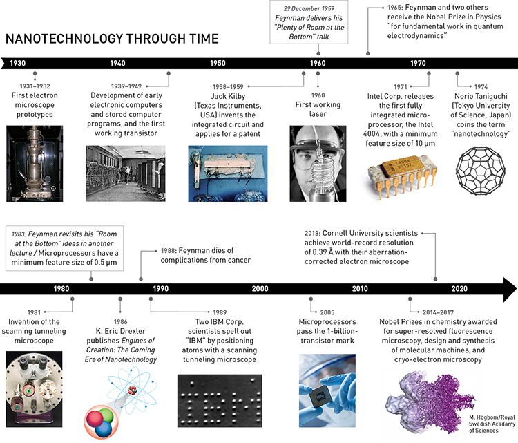 [Enlarge timeline] For further information/credits on the timeline photos, go online: www.osa-opn.org/link/bottom.
Tiny letters, shapes and bits
Decades before the internet era, the Encyclopedia Britannica was a standard summation of human knowledge in the English-speaking world. To introduce the “problem of manipulating and controlling things on a small scale,” Feynman proposed the notion of writing the encyclopedia’s entire text—filling 24 volumes in 1959—on the head of a pin. He took the notion of “text” literally; today’s readers of vintage encyclopedias would probably download the text in bits and bytes onto a thumb drive or SD card, and a commercially available version of the latter can store 256 GB in a space not much bigger than a postage stamp. Feynman, however, was interested in a literal inscription of the text as well as its digital translation.
To read those tiny words, Feynman suggested putting them under an electron microscope—which, to do the trick, needed more power and resolution. In the late 1950s, the instrument’s best achievable resolution was about 10 Å, which Feynman attributed to its small numerical aperture. He asked: Why must the field be axially symmetrical? Why must the field be stationary? Can’t we have pulsed electron beams in fields moving up along with the electrons?
“We’ve actually done that—we have broken the assumptions,” says David A. Muller, professor of engineering at Cornell University, USA, and co-director of the school’s Kavli Institute at Cornell for Nanoscale Science. “We no longer need the field to be symmetrical.”
According to Muller, electron microscopes hit a wall when simply directing more radiation through the instrument didn’t improve its resolution—it damaged the target. To increase resolution, scientists corrected the aberrations with powerful round magnetic lenses placed between the source and the sample. A scanning transmission electron microscope (STEM), like the one Muller uses at Cornell, makes multiple scans over a sample that is transparent to electrons. In time, these changes in technology have enabled STEMs to see down to 0.5 Å—a 20-fold increase since Feynman’s day.
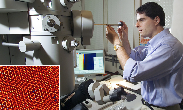 By adding ptychography to images taken with an aberration-corrected electron microscope, the team of Cornell University professor David A. Muller achieved a feature resolution below 0.4 Å. Inset: Ptychographic image of two sheets of molybdenum disulfide. [Cornell University]
Last year, Muller and his Cornell team set a world microscopy resolution record of 0.39 Å with electron microscope images corrected by ptychography: a computational imaging method based on translationally invariant interference patterns. The technique can be used with optical and X-ray imaging as well, according to Muller.
When discussing the miniaturization of information, Feynman did not ignore its digital representation. He posited that if we could make 100 atoms equal one bit—and he estimated that all the world’s books contained
1015 bits, or 1 petabit—we could store the world’s knowledge in a cube “one two-hundredth of an inch wide,” or 127 μm across. Given the growth rate of information over the past 60 years, it might be simpler just to visualize 1 petabyte (8 petabits) of information at Feynman’s ratio of atoms to bits—a cube merely 254 μm wide.
“That’s seriously thinking out of the box for his time,” Vahid Sandoghdar, director of the nano-optics group at the Max Planck Institute for the Science of Light, Germany, says of Feynman. But there’s still plenty of room to improve the bottom when it comes to inscribing tiny words. Electron-beam lithography can write small, and electron microscopy can detect patterns, but both methods are extremely slow. “You certainly wouldn’t want to read the Library of Congress using an electron microscope,” Sandoghdar adds. “That would take forever.”
Foreshadowing modern microscopy
Of course, today’s scientists have many more options than the traditional electron and light microscopes of Feynman’s day for peering into the very small. Feynman himself was still around when two physicists from IBM Research–Zürich, Switzerland, invented the scanning tunneling microscope (STM), which relies on quantum tunneling through the vacuum between the instrument’s tip and the target surface. The device can achieve resolutions of 1 Å, enabling scientists to see atoms.
In 1989, one year after Feynman’s death, Don Eigler and Erhard Schweizer of IBM Almaden Research Center, USA, made a splash when they used an STM to spell out their employer’s three-letter name in 35 individual atoms on a nickel surface. The feat took them some 22 hours.
Hot on the heels of STM technology came the atomic-force microscope (AFM), which entered the commercial market in 1989. The AFM works by measuring the short-range forces between the instrument’s cantilever tip and the surface atoms it scans, and it too can resolve and manipulate single atoms. AFMs also provide 3-D surface profiles, albeit with somewhat less vertical resolution.
Sandoghdar says that STMs and ATMs dominated nanotechnology in the early 1990s. His own field, the study of nanoscale light–matter interactions, did not emerge until later in the decade.
After several decades of chipping away at the diffraction limit, three scientists who developed super-resolution fluorescence microscopy techniques received the 2014 Nobel Prize in Chemistry. First out of the gate was stimulated emission depletion (STED) microscopy, which exploits the nonlinear response of fluorophores to achieve subdiffraction resolution. The ideas behind super-resolution microscopy have spawned several related techniques, including super-resolution optical fluctuation imaging and single-molecule localization methods, all used in molecular biology today. Feynman, who eventually succumbed to abdominal cancer, might have appreciated the resulting nanometer-scale views of the details inside individual cancer cells.
Shrinking the computer
In 1959, IBM Corp. introduced its 1401, a business-oriented mainframe computer with a CPU roughly the size of a home refrigerator. The 1401 had a magnetic-core memory; its input and output devices, such as a punch-card reader and a printer, were, judging from extant photos, at least as massive as the CPU.
Miniaturizing the electronic computer was another main theme of Feynman’s speech. He certainly didn’t predict the existence of pocket-sized computers like today’s smartphones, but he foresaw that circuitry had plenty of room to shrink. He predicted that computers would have wires 10 or 100 atoms in diameter, and circuits a few thousands of angstroms in length. In 1959, of course, the electronics industry was just pivoting from vacuum tubes to transistors, and the notion of a circuit completely integrated on a semiconductor wafer was in the patent-examination process.
 In the early 2000s, Chad Mirkin and colleagues at Northwestern University, USA, used dip-pen lithography to inscribe a nanoscale quotation from Feynman’s “There’s Plenty of Room at the Bottom” speech. [C. Mirkin / Northwestern University]
Today, the integrated circuits inside the latest smartphones are based on fin field-effect transistor (FinFET) semiconductor technology, in which current sources and drains are raised above the silicon substrate of the chip and connected with tiny “fins.” The first FinFET processors fabricated with the so-called 7-nm process rolled out of Taiwan Semiconductor’s foundry in late 2018, after several years of development. The next step in the semiconductor-manufacturing industry’s road map is the 5-nm process, but scientists and industry analysts are hotly debating how much further chip features can shrink without jeopardizing efficient fabrication.
Feynman couldn’t help mentioning in his lecture that the “microscopic” circuits in his brain were able to perform marvelous feats of facial recognition that the computers in the laboratories of his era could not. He thought a computer that could recognize faces might be as large as the Pentagon, and Earth might not contain enough germanium to make a computer that big. Information cannot travel faster than the speed of light, he added, so shrinking computers would speed them up.
Though several mathematicians took stabs at computerized facial recognition as early as the mid-1960s, the field burgeoned in the 1990s. Scientists continue to refine the technology even as it has become embedded in social media and security applications.
Miniaturizing machines
Fancifully, Feynman wondered out loud whether tiny machines could manufacture even more diminutive computers, or could become self-replicating factories. Today, artificial molecular machines still are nowhere near as complex as Feynman envisioned, and atom-by-atom manufacturing is not yet done on a commercial scale. In the laboratory, scientists are trying to make all sorts of tiny patterns and devices that, while they don’t resemble macroscopic tools, nevertheless possess scientifically important qualities.
The 2016 Nobel Prize in Chemistry went to three scientists who developed “molecular machines” out of molecules with certain shapes, such as catenanes (interlocked rings) and rotexanes (a dumbbell threaded through a ring). Scientists have known of the existence of these intriguingly shaped molecules since the 1960s, a few years after Feynman’s talk, but Jean-Pierre Sauvage (University of Strasbourg, France) and J. Fraser Stoddart (Northwestern University, USA) devised methods to synthesize these molecules and harness their properties to make molecular shuttles, cantilevers and self-replicators. Bernard Feringa (University of Groningen, Netherlands) made light-driven unidirectional motors from asymmetrical arrays of alkenes.
Cutting-edge research is reaching the point where scientists can fabricate wirelessly powered experimental robots small enough to be injected into a patient’s vein to monitor his or her vital signs—roughly the plot of the 1966 film Fantastic Voyage. Marc Miskin, an assistant professor at the University of Pennsylvania, USA, told this year’s APS March meeting that he and his Cornell colleagues built 70-μm-long robot bodies of silicon and glass, with platinum and titanium legs 100 atoms thick. So far the robots absorb energy from laser light, but that won’t work deep inside the human circulatory system; the team is exploring alternative means of powering the nanobots.
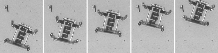 Researchers have created tiny functional, remote-powered, walking robots with legs just under 100 atoms thick and powered by laser light hitting the robots’ solar panels. Smart versions of the robots could potentially make incredible journeys in the human body. [M. Miskin / Univ. Pennsylvania]
Astoundingly, Feynman predicted the existence of one hot topic of today’s research landscape that had no name in 1959. He asked: Suppose one had built an array of circuits a few hundred to a thousand angstroms in size, connected to a field of tiny antennas—could the array beam out high-intensity light? Such artificially created nanopatterns manipulate light today. We call them metamaterials.
Scientists started discussing the concept of an optical antenna only around 2000, and it emerged out of near-field optics, Sandoghdar says. “The amazing thing for Feynman was to have had such insight,” he adds, since he was speculating outside of his usual discipline of theoretical particle physics.
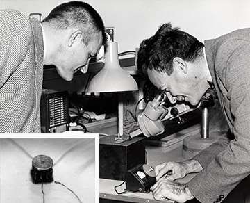 Feynman (right) offered a US$1,000 prize to the first person to make a motor that would fit into a 1/64-inch cube. In 1960, William McLellan (left) designed a motor only 15/1000 inch in diameter (inset). [Caltech Archives / Photograph used with the permission of Melanie Jackson Agency, LLC]
Legacy of Feynman’s talk
In the conclusion to his 1959 speech, Feynman challenged people to build a working electric motor that would fit into a cube 1/64 inch (0.04 cm) across. Less than a year later, a Caltech engineer named William McLellan built just such a device, enclosed in a container with a magnifying glass to make the motor visible and a knob to crank a small generator to run the motor. Feynman’s other 1959 challenge—printing letters 1/25,000 the size of the characters in a book—took longer to realize, but in 1985 a graduate student, Tom Newman of Stanford University, USA, carved out the tiny text using electron-beam lithography.
In 1983, as his original address was nearing its quarter-century anniversary, Feynman reviewed the state of nanoscience during a lecture at the Jet Propulsion Laboratory, USA (later transcribed for publication). The state-of-the-art computer-chip technology of the time had a resolution of about 0.5 μm, which was the best scientists could do with light, he opined.
Feynman still didn’t think that micro-machines would have any use, and with tongue firmly in cheek, he professed that he couldn’t explain why they fascinated him. Nevertheless, as he discussed semiconductor fabrication, he correctly predicted that computer circuitry would have to move from two to three dimensions—presaging such structures as FinFETs. He also insisted that, since atoms obey quantum rather than classical rules, computational circuits on the atomic scale would have to employ reversible gates.
Although, in hindsight, Feynman has been credited with sparking interest in nanotechnology, historians of science generally say that the field started in the 1980s and 1990s and retroactively appropriated the Nobel laureate’s musings as a stamp of authenticity. Molecular-machinery advocate K. Eric Drexler took the concepts of Feynman’s talk and expanded on the notion of self-replicating nanorobots in his 1986 book Engines of Creation: The Coming Era of Nanotechnology. Between that book and Feynman’s death, the 1959 lecture, which had been little cited, found a new audience.
OSA Fellow Alexandra Boltasseva, an engineering professor at Purdue University, USA, says she first learned of Feynman’s talk in an introductory graduate-level course on nanotechnology. Recently, as the 60th anniversary of “Plenty of Room at the Bottom” has drawn near, she asked her Purdue undergraduate students to read the text of the speech as a class assignment. She was fascinated to hear their opinions on the ideas they connected with: atom-by-atom manipulations, information density, even drug delivery.
Odom says society needs “colorful people who will go out on a limb and talk about a huge range of topics—which shows you how inclusive [Feynman’s] views of science and physics were—and touch points related to technology, which physicists don’t like to talk about much.”
Sandoghdar says he’s still pursuing his ultimate goal of sculpting light at the single-photon level. Some of the hot topics of quantum optics, like squeezed light and entangled photons, are still rudimentary and for lab use only, but they may form the basis of the next wave of hot technology.
These days, it’s rare to catch a glimpse of OPN’s website when its home page does not include words like “nano,” “quantum” or “metamaterial.” Unimaginably small objects and atomic-level details are now part of the optical scientist’s toolbox. After six decades of innovation, there is still room at the bottom.
Patricia Daukantas is a freelance science writer based in Greenbelt, Md., USA.
References and Resources
-
R.P. Feynman. “There’s plenty of room at the bottom,” California Inst. of Technol. J. Eng. Sci. 4(2), 23 (1960). Reprinted in J. Microelectromech. Syst. 1(1), 60 (1992).
-
R.P. Feynman. “Infinitesimal machinery,” J. Microelectromech. Syst. 2(1), 4 (1993).
-
J. Gribbin and M. Gribbin. Richard Feynman: A Life in Physics (New York: Plume, 1998).
-
D.A. Muller. “Structure and bonding at the atomic scale by scanning transmission electron microscopy,” Nat. Mater. 8, 263 (2009).
-
M. Segal. “Surely you’re happy, Mr. Feynman!,” Nat. Nanotech. 4, 786 (2009).
-
B. Le Bailly. “Welcome to the machine,” Nat. Nanotech. 11, 923 (2016).
-
S. Shankland. “IBM’s 35 atoms and the rise of nanotech,” www.cnet.com/news/ibms-35-atoms-and-the-rise-of-nanotech/ (28 September 2009).
-
S. Shankland. “Samsung promises four generations of new chip technology,” https://www.cnet.com/news/samsung-promises-four-generations-of-new-chip-technology/ (22 May 2018).
-
M. Henstridge et al. “Synchrotron radiation from an accelerating light pulse,” Science 362, 439 (2018).