
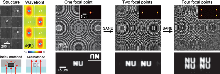
 Left: Wavefront phase tuning by patterning dielectric blocks on arrays of plasmonic nanoparticles. Middle and right: Metalens reconfiguration from a single- to multi-focal designs by solvent-assisted nanoscale embossing, and the corresponding images formed from a “NU” pattern. [Adapted from reference 2.]
Compact optical components are crucial for miniaturized imaging systems that can be integrated into portable devices. Metalenses1 are emerging as a class of planar structures that can focus light by tailoring the optical wavefront with nanoscale units. With feature heights of less than a micron, metalenses have been used in devices ranging from compact endoscopes to wide-angle cameras. Existing metasurface lenses made of hard materials, however, have fixed optical responses and cannot adjust the foci over multiple image planes; adaptive metasurface performances will require a reconfigurable materials system. This year, we demonstrated such a system using plasmonics.2
Plasmonic nanoparticle arrays that support surface lattice resonances (SLRs) are promising for achieving metalenses with dynamic responses, because these plasmon excitations produce abrupt phase delays at resonance and can be tuned by changing the dielectric environment.3,4 Lensing by SLRs has not yet been reported because existing methods cannot tune the wavefront phase between adjacent nanoparticles in the array.
We demonstrated a materials platform for realizing metalenses with unit-level reconfigurability for imaging at visible wavelengths.2 The lenses were built based on two elements arranged in a square lattice: (1) silver nanoparticles exposed to air, and (2) identical particles covered by a thin dielectric block. This plasmonic array was designed to support surface lattice resonances in a uniform dielectric environment where the media surrounding the nanoparticles all have the same refractive index. When covered by patterns of polymer resist, prominent wavefront intensity and phase changes were observed only on nanoparticles in the resist blocks whose index matched the silica substrate.
We realized large-area metalens reconfiguration by re-forming the dielectric blocks on the nanoparticles by a technique called solvent-assisted nanoscale embossing,5 which we had developed in 2011. During lens reconfiguration, the single-step embossing process erased the existing polymer patterns and redistributed them into the designs defined on the PDMS mask. This strategy could reversibly switch the resist pattern between two or more lens designs with no observable degradation in the nanoscale feature quality.
Finally, we showed how this materials platform can be applied to adaptive lensing by evolving a lattice-resonance metalens sequentially from a single- to multi-focal point configurations during the same experiment. We believe that the resulting tunable metalenses can potentially realize next-generation imaging systems with unprecedented compactness.
Researchers
Jingtian Hu, Danqing Wang, Debanjan Bhowmik, Tingting Liu, Shikai Deng, Michael P. Knudson, Xianyu Ao and Teri W. Odom, Northwestern University, Evanston, Ill., USA
References
1. M. Khorasaninejad et al. Science 352, 1190 (2016).
2. J. Hu et al. ACS Nano 13, 4613 (2019).
3. S. Zou et al. J. Chem. Phys. 120, 10871 (2004).
4. V.G. Kravets et al. Nat. Mater. 12, 304 (2013).
5. M.H. Lee et al. Nano Lett. 11, 311 (2011)