
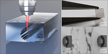
 Left: Femtosecond laser lithography in polycrystalline diamond. A tightly focused laser pulse induces a material modification forming the boundary of the diamond waveguides. Top right: Processed diamond chip with numerous waveguide structures. Bottom right: Sample end-facet showing the induced waveguide structures and the guided near-field mode profile as an overlay. [Enlarge figure]
Diamond photonics is helping to drive the second quantum revolution and to break new ground in biological applications, nonlinear photonics and optoelectronics.1 However, for many years integrated diamond photonic systems have been limited to quasi-planar geometries and thus not considered for 3-D photonic networks. This year, we used femtosecond laser lithography to fabricate 3-D waveguide structures on a polycrystalline diamond platform as a first step to such a photonic network.2
New fabrication routines based on direct laser writing have recently been employed to integrate a 3-D optical system on a monocrystalline diamond platform.3 However, the challenges in fabricating large-scale monocrystalline diamond substrates limit this method’s application considerably. Polycrystalline diamond substrates, in contrast, can be reproducibly manufactured in wafer-like sizes with high optical quality, to satisfy the demand of large-scale 3-D diamond photonic system.
Large-scale polycrystalline diamond substrates are already widely used for high-power infrared and microwave windows, or as heat spreaders in high-power integrated circuits. Furthermore, the ability to grow large-area polycrystalline diamond thin films on diverse insulating substrates—for instance, SiO2—makes them attractive for on-chip photonic circuits, and opens the field for diamond-based surface-acoustic-wave devices for wireless communication systems and applications in sensing.4
In our recent work, we were able to use femtosecond laser lithography to successfully integrate complex 3-D waveguide structures onto such a polycrystalline diamond platform.2 A tightly focused infrared laser beam modifies the diamond substrate in a highly localized way within the focal volume. Translating the substrate relative to the beam focus allows the induction of 3-D, micrometer-scale structures.5 The fabricated waveguides feature good light-guiding properties in the near-infrared telecom C-band. Furthermore, we demonstrated the versatility of our approach to fabricate photonic structures with arbitrary geometry within the diamond substrate.
We believe that our technique paves the way to implement advanced diamond photonic networks on large-scale polycrystalline diamond substrates. Our findings also could achieve the long-standing goal of fabricating true 3-D, large-scale photonic circuits on diamond—making its outstanding optical properties accessible for computational on-chip devices. This should open up applications in classical and quantum photonic systems in areas including telecommunications, metrology and sensing. Ultimately, we believe that this work could spawn a new field, diamond integrated on-chip solutions, that offers many advantages—for instance, the combination of optimized photonic building blocks with small footprints and an increased bandwidth with low-loss signal transmission.
Researchers
Haissam Hanafi and Cornelia Denz, University of Münster, Münster, Germany
References
1. I. Aharonovich et al. Nat. Photon. 5, 397 (2011).
2. H. Hanafi et al. Opt. Mater. Express 9, 3109 (2019).
3. V. Bharadwaj et al. J. Phys.: Photon. 1, 022001 (2019).
4. F. Lenzini et al. Adv. Quantum Technol. 1, 1800061 (2018).
5. S. Kroesen et al. Opt. Express 22, 23339 (2014).